Other Parts Discussed in Thread: AFE58JD48, , LMK04826
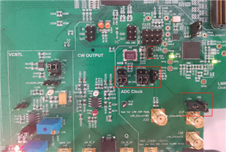
We are currently evaluating the AD acquisition performance of the AFE58JD48 chip with AFE58JD48EVM. However, we have no EVM related to TSWxxx. We use the FMC interface of the zcu106 (Xilinx EVM) to connect to the AFE58JD48EVM, The jumper configuration of AFE58JD48EVM is as follows:
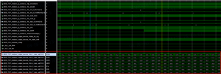
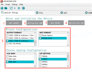
Follow these steps to set it
The result of measurements are as follows:
- LMK_ADC_CLKP--TP44: average voltage is about 1.25V,frequency is about 322MHz,Vpp is about 200mV.
- FPGA_CLK_OUT_P has no clock
- CLK_GTXP: average voltage is about 1.25V,frequency is about 119MHz
- FPGA_SYSREFP: average voltage is about 1.239V,frequency is about 2.5MHz;
My questions are :
- Why do all the clocks measured above have a DC bias of about 1.25V? Is it normal?
- According to the AFE58JD48EVM_User 's_Guide and the configuration of jumper, the AFE clock is either 125MHz or 40MHz, but the TP44-LMK_ADC_CLKP measured is 322MHz. How is this?
- Why does FPGA_CLK_OUT_P have no output clock? Is this clock the glblclk or rx_core_clk corresponding to the JESD204B interface?
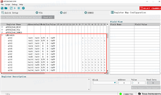
- What do 120M and Dec in the following configuration mean? What should I do if I want to modify JESD parameters? For example, set it to JESD Subclass 2, or change the clock of JESD.
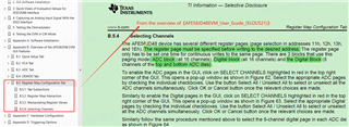
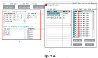
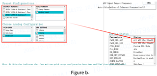
- Why can configuration 1 and configuration 2 in Figure a not exist at the same time? In Figure b, after the parameters in Preset Configurations are configured, the Device Status displays All ADC CHs Disable. In this case, can the ADC output data normally?
Thank you very much for your reply !