This thread has been locked.

If you have a related question, please click the "Ask a related question" button in the top right corner. The newly created question will be automatically linked to this question.

ADS8862: RC filter for ADC input

Part Number: ADS8862
Other Parts Discussed in Thread: TLV9102, REF6050, REF5050, OPA320, ADS8860

Dear Technical Support Team,


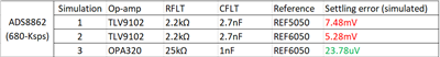
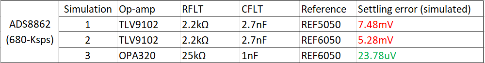
ADS8862 datasheet shows Charge-Kickback Filter and RFLT 22Ω and CFLT 590 pF(Figure 62. Charge-Kickback Filter), but my configuration is simply RC filter for ADC driver with TLV9102.


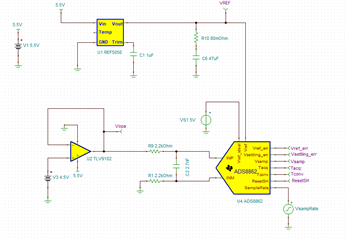
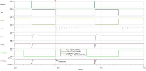
I posted for TLV9102(buffer) with R=2.2kΩ and C=2,700pF for RC filter and attached file(block diagram)

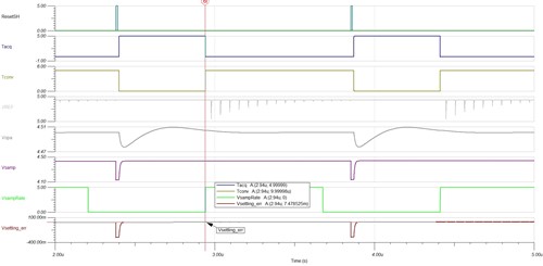
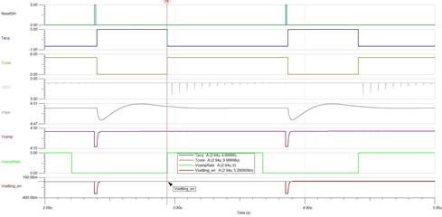
I'm confirming the phase margin and stability on followingE2E.


https://e2e.ti.com/support/amplifiers-group/amplifiers/f/amplifiers-forum/1305637/tlv9102-output-oscillation-issue-with-cl

Attached file 

TLV9102_ADC.pdf 

I would like to confirm whether there is no problem with ADS8862 even if the configuration and constants are different between Figure 62. Charge-Kickback Filter and my board's RC filter.

Also, please let me know if you have any ideas or recommended constants for a simple RC filter.


Best Regards,


ttd

  • Hi ttd,

    The series resistor (RFLT) used at the output of the amplifiers can avoid amplifier stability issues, however a higher value of RFLT adds distortion as a result of interactions with the nonlinear input impedance of the ADC and it will affect the performance of your system.

    Below are simulations I just did. As you can see from the simulation result, the circuit 1 showed the largest settling error (7.48mV vs. 1LSB=76uV for 5V FS), the circuit 3 is recommended which used the recommended value for RFLT and CFLT and showed a small settling error 23.78uV, and also REF6050 is recommended because it has integrated a reference buffer. When REF5050 is used, an external reference buffer is needed especially at higher sampling rate.

    Notice that the simulations were done with the highest throughout 680-kSPS for ADS8862 ADC. When the actual sample rate is reduced, the requirement for front-end driving circuit is relieved too. You can also see unstable output from TLV9102 in the simulation result, the output signal from OPA320 op-amp is more stable that other two circuits. OPA320 works well, but you can also check with the amplifier team in your another query for their recommendation, a higher BW op-amp is needed especially when your ADC works at a higher sampling rate.

    Summary: 

    Simulation 1:

    Simulation 2:

    Simulation 3:

    Best regards,

    Dale

  • Hi Dale,

    Thank you for your reply.

    ①Is it possible to attach three TSC files you simulated?

    ②Unfortunately current circuit is simple RC filter(Not Charge-Kickback Filter), If I change only R1 from 2.2kΩ to 0Ω and simulate it, can I check the settling error?

    ③Also VsampRate seems to set 680ksps. 

    Is it correct to understand that lowering the sampling rate will alleviate the settling error? I would like to check what SPS is better to lower the settling error as much as possible with the current circuit configuration.

    Best Regards,

    ttd

  • Hi ttd,

    See my feedback below:

    1. You can directly download the TI-TINA model and simulation file from the product folder on TI.com, see ADS8862 simulation file here, then modify it according to your actual circuit. I also upload one file in the following link:

    /cfs-file/__key/communityserver-discussions-components-files/73/ADS8862_2D00_REF5050_5F00_TLV9102.TSC

    2. The filter here is a charge bucket filter ( also called charge-kickback filter). You can modify RC value in the simulation file and check the settling error.

    3. You can modify the throughput in the simulation file and simulate it again if needed. 

    Your understanding is correct.

    Regards,

    Dale

  •  Hi Dale,

    Thank you for your support.

    According to your summary of settling error, RFLT=25kΩ of charge-kickback filter for Simulation 3.

    How do you calculate it? Is the correct value  RFLT=25Ω?

    Figure 62. Charge-Kickback Filter shows RFLT 22Ω and Figure 63. DAQ Circuit for a 1.5-µs, Full-Scale Step Response shows  RFLT=15Ω and CFLT=1nF.

    Could you advice it?

    Additional Question for REF6050.

    RLIMT for SS pin, ADS8862 datasheet shows 5mΩ(0.15mA) but REF6050 datasheet shows 120kΩ(3mA).

    I use following Equation from REF6050 datasheet.

    ADS8862 datasheet shows Reference input current =160uA(typ). 

    Is it necessary to set the output current of REF6050 with SS to 160uA or more?

    Best Regards,

    ttd

  • Hi ttd,

    Please see my answers below:

    1. RFLT:  it's a typo, it should be 25Ω which was used in my simulation. Sorry for the confusion to you.

    2. The combination of Cflt and Rflt affect the settling result. The value of Rflt can be used as long as the settling error is less than 0.5LSB with your selected Cflt. My simulation has shown a good result with 25Ω Rflt and 1nF Cflt.

    3. The current should meet the settling requirement for ADC. The smaller value resistor on SS pin of REF6050, the less current from the reference. I used 120kΩ (3mA setting) on SS pin of REF6050 and did not see any issue when I used REF6050 for ADS8860 (1Msps ADC) in the past.

    Regards,

    Dale

  • Hi Dale,

    Thank you for your reply.

    I got your answer.

    I have other question.

    For example, if the ideal value of the ADC input is 1V, is it correct to understand that Vsettling Error includes a direct error and is converted into a code as 1V+Vsettling Error?

    Also, is Vsettling Error the worst value including PVT?

    This training video page 14 shows Error Target = 38µV Simulate Error = -41mV on output.

    https://www.ti.com/content/dam/videos/external-videos/2/3816841626001/5752954742001.mp4/subassets/amplifier-settling-lab-presentation.pdf

    Best Regards,

    ttd

  • Hi ttd,

    I do not understand your questions. The settling error is the difference between the actual input and the settling signal on internal S/H capacitors. The actual code you get from the ADC includes all errors (offset error, error caused by power supply ripple and so on). I would suggest you to go through the whole series of Precision Labs - Input Driver Design.

    Regards,

    Dale

  • Hi Dale,

    Thank you for your answer.

    I watch training video to learn settling error.

    I tried to compare with 680ksps and 340ksps with OPA320 + RC Filter.

    Because it's easy to change on my board pattern(AW). In my case, it is necessary to do pattern cut and wire jumper  for changing Charge kickback filter.

    Is this the limit to accuracy improvement with this circuit configuration?

    ADS8862-REF5050_OPA320_RC.TSC

    Best Regards,

    ttd

  • Hi ttd,

    Your simulation file was configured with 100ksps sampling rate not 680ksps or 340ksps, and also I did not understand your question and your concern. If your components including RC, op-amp and reference are not properly selected, you will get poor performance including DC performance (the "accuracy" you are talking) and AC performance (THD). Once the components are properly selected for 680ksps sampling rate, your system will operate at 340ksps sampling rate without any issues.

    I'm going to close this thread if you do not have other question.

    Regards,

    Dale