This thread has been locked.

If you have a related question, please click the "Ask a related question" button in the top right corner. The newly created question will be automatically linked to this question.

DAC11001A: Output Voltage Settling Time Min/Max?

Part Number: DAC11001A

Hi all, 

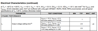
I am looking into the DAC11001A's output voltage settling time parameters. However, only the typical time is provided, and I was wondering if there is any data available for the min/max settlings times of the part based on the input conditions stated in the datasheet. 

Thank you

Thank 

  • Hi Filipe, 

    Akhilesh should be able to check to see if any additional data exists and will get back to you soon. 

    Best,

    Katlynne Jones

  • HI Filipe,

    We do not really have min/max data as this is highly dependent on the external amplifier, external load, and some settings for the track-and-hold circuit in the DAC11001A.  Completely unbuffered with no output loading, the settling time would be <1us regardless of voltage step size.  But, as that would be a very useful configuration, I think you should instead look at the output buffer you would like to use and evaluate their settling time specification.  Our dac's output impedance is ~6.25kohm, and we will have some parasitic capacitance on the pin, so that will slow the transient slightly.  Otherwise, we have our track and hold circuit delay, which is <1us.

  • Hi Paul, 

    Thank  you for letting me know. In a similar vein of question, do you know how much the settling time would be improved if I set the FSET bit to 0 as described below in section 8.4.1 of the datasheet? Or is this dependent on external factors?

    The DACx1001 R2R ladder and deglitch circuit reduce the harmonic distortion for waveform generation applications. The fast settling bit (FSET, bit 10, address 02h) is set to 1 by default, so that the DAC is configured for enhanced THD performance. The FSET bit can be reset to 0 using an SPI write to enable fast-settling mode. In this mode, the DAC deglitcher circuit can be configured using TNH_MASK (bits 19:18, address 02h). These bits disable the deglitch circuit for code changes specified in Table 7. These bits are only writable when FSET = 0 (fast settling enabled) and DIS_TNH = 0 (deglitch circuit enabled).

  • Hi Filipe,

    The FSET=0 mode means that the TnH is disabled when the code steps are greater than the limits set by TNH_MASK.  The idea being that when the code step of the output is large, the THD contribution of glitch is less critical than any THD caused by the output not settling before the next code is written.  The UP_RATE field sets the TnH default time, generally on the order of ~100-700ns.  It assumes we have a constant sample rate.

    I think the best way to optimize the settings for your application is to determine the maximum code step you expect for a given update rate and output tone.  If you see code steps in the range of the TNH_MASK settings, you should implement the FSET function.