Hello everyone,
My ADC (16 bits) returns values that seem to be off by half the resolution. For example, by configuring input AIN0 as AINp and AIN1 as AINn, I get results such as:
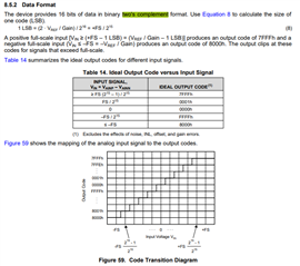
- AIN0 = AIN1 = GND, Expected value: 0, Value given by ADC: 0
- AIN0 = Vref, AIN1 = GND, Expected value: Vref, Value given by the ADC: 32767
- AIN0 = GND, AIN1 = Vref/2, Expected value: -Vref/2, Value given by ADC: 49 152
- AIN0 = GND, AIN1 = Vref, Expected value: -Vref, Value given by ADC: 32768
- AIN0 = Vref, AIN1 = GND, Expected value: 0, Value given by ADC: 0
Values are coded from 32768 to 32767, starting with 0.
Similarly, when configuring a single-ended input:
- AIN0 = GND, Expected value: 0, Value given by ADC: 0
- AIN0 = Vref, Expected value: 65535, Value given by ADC: 32767
The weird thing is that I was basically getting the output right, so I'm sure the answer is quite simple...
I'm also pretty sure that the ADC doesn't have a sign bit.
Here is the configuration I used:
#define REG0_AIN0_AIN1    (CONFIG0_MUX_AIN0_AIN1 | CONFIG0_GAIN_1 | CONFIG0_PGA_BYPASS_YES_DISABLED)
// #define REG0_AIN0         (CONFIG0_MUX_AIN0_AVSS | CONFIG0_GAIN_1 | CONFIG0_PGA_BYPASS_YES_DISABLED)

#define REG1              (CONFIG1_DR_20_SPS | CONFIG1_MODE_NORMAL | CONFIG1_CM_CONTINUOUS | CONFIG1_VREF_INT | CONFIG1_TS_DISABLED)
#define REG2              (CONFIG2_DRDY_OLD | CONFIG2_DCNT_DISABLED | CONFIG2_CRC_DISABLED | CONFIG2_BCS_DISABLED | CONFIG2_IDAC_OFF)
#define REG3              (CONFIG3_I1MUX_DISABLED | CONFIG3_I2MUX_DISABLED | CONFIG3_AUTO_MANUAL)
#define REG4              (CONFIG4_GPIO2DIR_OUT | CONFIG4_GPIO1DIR_IN | CONFIG4_GPIO0DIR_IN | CONFIG4_GPIO2SEL_DRDY | CONFIG4_GPIO2DAT_LO | CONFIG4_GPIO1DAT_LO | CONFIG4_GPIO0DAT_LO)
Thanks for your help