This thread has been locked.

If you have a related question, please click the "Ask a related question" button in the top right corner. The newly created question will be automatically linked to this question.

ADS131M06: sampling synchronization question

Part Number: ADS131M06

Hi team,

I plan to recommend ADS131M06 to my customer, could you help check these questions for me ?

1. Is the current life cycle of ADS131M06 recommended for new designs?

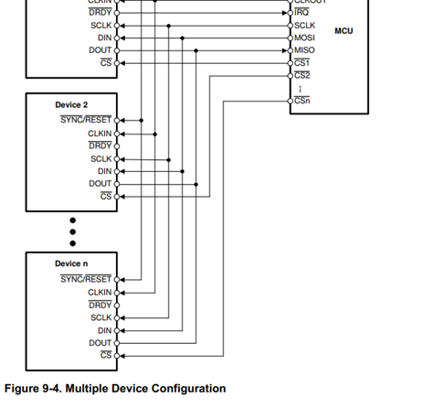
2. If you want to use three ADS131M06 chips for multi-channel sampling, how to achieve sampling synchronization of 3x6 = 18 channels? To achieve sampling synchronization, must all ADCs be based on the same clock source? How long does it take from SYNC/RESET to change to 1 until ADC starts sampling?

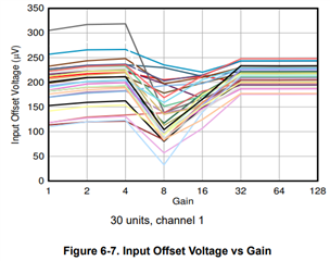
3. The Offset error parameter in the datasheet only provides two typical values. Does ±240 correspond to Continuous Conversion Mode? What is the maximum value of Offset error? If you change the Gain setting, will the Offset error also change?

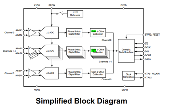
4. Our application scenario is to input a current signal of 5mA – 300A. Can ADS131M06 complete data acquisition by adjusting the internal PGA without an external amplification circuit? 

Thanks

Lillian

  • Hi Lillian,

    Thank you for promoting PADC, please see the answers below:

    1. Yes, ADS131M0x is a very popular ADC and it can definitely be promoted for a new design.

    2. The /SYNC/RESET pin can be used to synchronize conversions between multiple ADS13106 ADCs as well as to maintain synchronization with an external event. Yes, the same clock source should be used and also the customer should pay more attention to their pcb layout to minimize any impact to the clock signal to these ADCs. After the ADCs are synchronized, internal digital filters require time to settle, see the settling time vs. OSR in the table 8-3 of the data sheet.

    3. Yes. Also, +/-32uV is typical offset voltage in global-chop mode. The maximum spec was not characterized, however a mean + 6 sigma number can be used as a idea of a maximum value for evaluation purpose. There are some variation in offset voltage (input referred) across gain, see Figure 6-7 in the data sheet:


    4. You did not mention the shunt resistor value, but generally the answer is yes as long as the customer can select a proper value of shun resistor according to the gain range of ADS131M06 ADC.

    Best regards,

    Dale

  • Hi Dale,

    Thanks for your detailed reply.

    We still have some questions below, pls help:

    1. 

    I realize the clock signal is very important for synchronization between multiple ADS131M06.


    Because figure 9-4 in the datasheet shows multiple device configuration, I guess there is some recommended solution about how to prove clock for multiple ADS131M06 from Ti.

    Could you share more information about the solution of clock source? Is a clock buffer required for below application?

    2. 

    I have two more questions about the block diagram of ADS131M06:

    Why isn’t Gain setting in front of ADC?

    Is there any difference between channel0/5 and channel 1-4? (Channel 1-4 are in same group according to above figure)

    Thanks Lillian

  • Hi Lillian,

    Customers can provides a master clock from their MCU/FPGA or a standalone oscillator for all ADCs (e.g.  SIT8924BA-22-33E-8.192000G which has been used and verified on ADS131M08EVM). A clock driver will be helpful to drive more ADCs. If the driver is very weak, the CLKIN pin will be more susceptible to any disturbance compared to the case when the driver is strong.

    The gain can be set in GAIN1 and GAIN2 registers for all channels. It is a capacitive gain stage. This is just a block diagram and there is no difference between these channels in terms of gain stage.

    Regards,

    Dale