This thread has been locked.

If you have a related question, please click the "Ask a related question" button in the top right corner. The newly created question will be automatically linked to this question.

ADS8664: ADS8664 Analog Input Readings Get Intermittently Stuck at Last Read Value

Part Number: ADS8664

Hello,

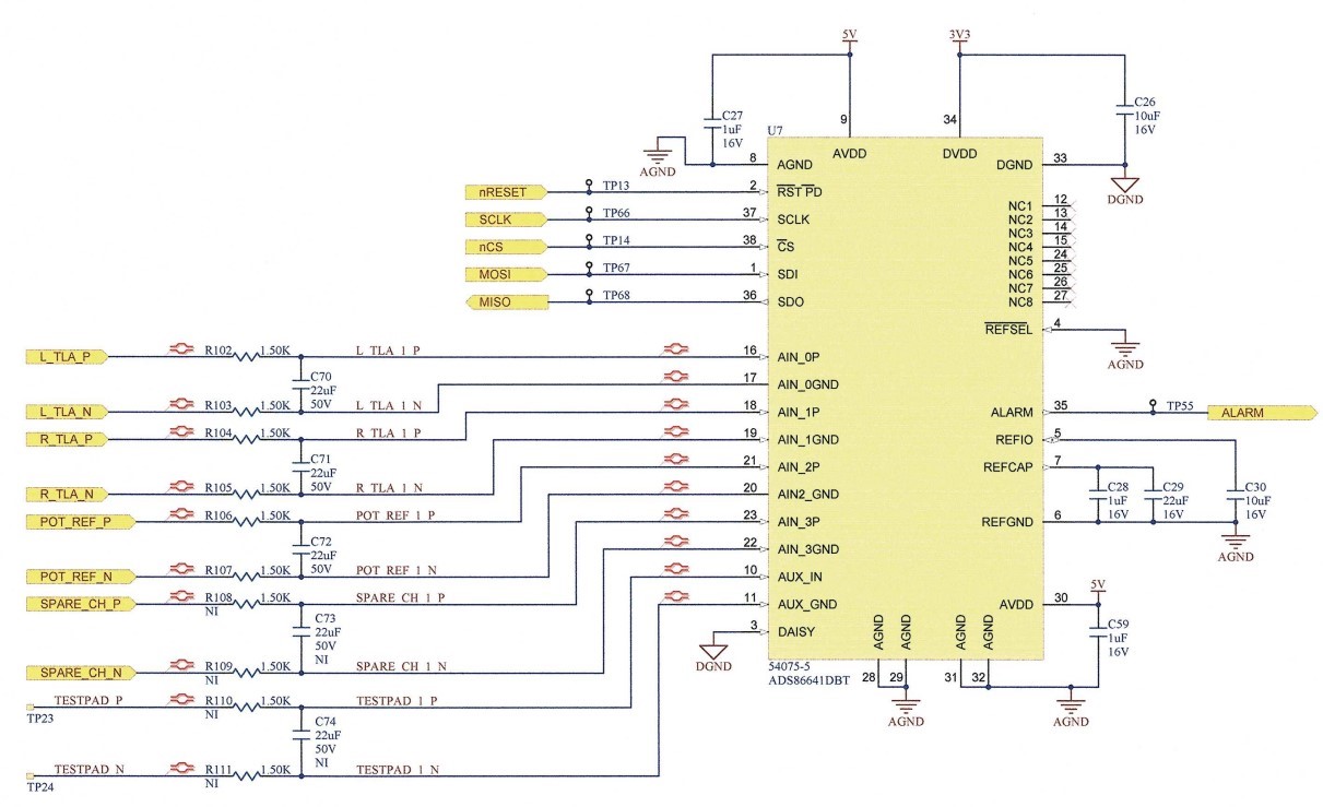
I am using the ADS8664 for 4 analog input signals in one of my designs (schematic below). The problem I am having is that the ADC input gets locked up intermittently. I have checked the SPI output to ensure that the receiving microcontroller isn't the device getting locked up, when using a logic analyzer I can see that the SPI messages are healthy and do indeed repeatedly output the same message. This would imply that the ADS8664 is getting "stuck" internally somehow.

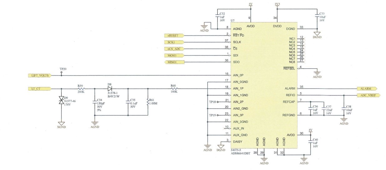
The error will sometimes clear with a power cycle, though not consistently; this is slightly more consistent when I disconnect the main harness connector to the unit. The error has cleared itself while the unit was running, though this has been rare. The voltage range of the inputs is roughly -10V to 10V. We have used this device on two other designs with an effectively identical supporting components and no issues, the only difference I found was that we grounded REFSEL to our AGND plane (analog ground section) on the other designs. As you can see below I grounded this chip to our DGND plane (digital ground section). The data sheet states "In order to select the internal reference, the REFSEL pin must be tied low or connected to AGND." This "or statement" is confusing, as tied low could imply DGND. In any case, I tried lifting the REFSEL pin and jumpering it to AGND in case there were noise issues, but the issue persisted; however, I am not sure if the speed wire would be efficient for this rework if the issue is digital/analog noise effecting the other side of the internal circuitry.

This issue has shown itself on multiple units in the same fashion, so unless this is a "chip lot" malfunction issue, I have proven that simply replacing the chip does not fix the issue. I am out of ideas for troubleshooting the chip itself, and wondering if I should start investigating other areas of my circuit board. I am also wondering if at this stage, if the circuit looks good, I can start to push the software team to troubleshoot from a programming angle, perhaps timing issues? That area is out of my element.

Any suggestions to help me home in on a solution would be greatly appreciated.

Thank you for your time!

  • Hi Keith,

    I see three different grounds in your schematic.  All three of these should be tied together somewhere, ideally near the ADS8664.  How does your layout look wrt the various ground pins?

  • I double checked this and DGND and AGND basically via down at their pins to the layer below and are grounded in the same plane, which takes up the whole layer. The CH_GND is for the lightning protection diodes only, there is a plane under the mounting holes around the edge of the board about an inch from the ADS8664. The net tie that connects CH_GND and DGND connects with a bidirectional leveling diode on the side of the board opposite the ADS8664. The aforementioned DGND plane is poured across an entire layer of the board. Thank you!

  • Hi Keith,

    What about transients?  Are there any transient events that cause AGND and DGND to shift?  Any brownout condition on AVdd or DVdd?

  • I haven't been able to observe any obvious power issues or brownout conditions and I have confirmed that Vref (REFIO pin) is at a steady 4.093V when in the "locked up" state.

    I was considering setting up a scope/data logger that can show if there is any Voltage "event" that happens when the chip gets stuck, but I don't have an immediately obvious way to make that recording happen.

    I will say, we have confirmed that this issue shows itself in our verification testing, when the verification test cycles power frequently, however I have ensured that it is impossible for the 5V rail to come on before the 3V3 volt rail (since it feeds the 3V3 regulator). There is also a 50ms delay before the 3V3 regulator is enabled, meaning the ADC turns on after our microprocessor which is on its own regulator. Not sure what kind of startup sequence may fix this issue, but a longer delay did not seem to help. Could powering the chip down with the input voltage present cause something to latch? 

    Thank you!

  • Hi Keith,

    Having voltage on the inputs while cycling power could certainly cause issues.  You can back drive through the ESD cells which could put the part into an unknown state (i.e. latched up), potentially causing damage to the device.

  • This is very helpful, I'll use your account to encourage the software guys this might be a problem and let you know. 

    Thanks!

  • Tom,

    I had the software team make sure that the function generator was shut off before cycling power to the chip, and it did not prevent latch ups. I also had them try to set the function generator to 0V before cycling power to the chip and the results were the same.

    Is there anything about the schematic I posted in my original prompt, on either the input path or grounding scheme of AGND vs DGND (which going into the same plane) that could be the culprit? Basically, would you be surprised if my grounding scheme was causing the issue?

    I am otherwise very much at a loss here, unless the chip is damaged. I haven't replaced the chip with a new one yet since it functions fine without power cycle before it gets latched up.

    Thank you!
    Keith

  • So, from the original post, your schematic shows AINx_GND going off page.  This input is normally tied to AGND, so are you terminating that somehow?  Also, the 20uF of capacitance on the inputs seems quite large - are those caps getting discharged between power cycles?  Ideally AUX_IN would terminated, but I don't think that would cause the part to latch up.  You mentioned that you used the ADS8664 in a previous project - can you share the delta's from the design/schematic and layout differences?

  • Regarding the AINx_GND, those Aux pins have been left floating at the pad. The ALARM pin going off page is connected to a GPIO on the microprocessor

    Here are two other designs that we have not observed this exact issue with. It appears we ground aux on one but not the other. One design has similar inputs with 22uF caps, the other is different since it is connect to a linear transformer. 

    Thank you!

  • Hummm... running out of ideas here.  Does toggling RST/PD bring the part back to life?  If you set the pin low before cycling power, does that help?

  • The RST pin is tied to a RST bus from the microprocessor that many devices on the pcb use. I can try giving this its own dedicated GPIO port so software can experiment with cycling power with RST in different states.

    Revisiting DGND vs AGND. I can remove the IC and set up a "daughter board" with a new chip where the GNDS are totally separate (since the PCBoard can't be modified due to the vias and buried ground plane). Do you think this would be worth testing? It would just require quite a bit of reworking and I'm worried that if it is in fact that sensitive to this sort of thing it'll be moot anyway. 

    Thank you!

  • Hi Keith,

    To be honest, I'm not sure that pulling off the chip and trying to re-work it in situ is going to help - that might bring more questions than answers.  Let's try the RST/PD pin thingy first and then perhaps we can get on a conference call and review your layout details before trying to do a daughter board.

  • Hello!

    I tried triggering the RESET pin manually, and it did not appear to clear the stuck fault. Weirdly enough, it seems like it pulls all of the inputs high, or low to the maximum input voltage (+/-10.24V), following whether or not the GPIO to the RESET pin is set high or low.

    Now, we tried again only this time I grounded both AUX_IN and AUX_GND to DGND, with the reset pin pulled low (it is an nRST pin) it appears to put the ADC in reset, with a value of -10.24V (which is all 0s digitally). When set high, the ADC runs and the value appears to be unstuck. For a moment I was hoping that grounding the floating AUX inputs was the solution, but when I dropped the RESET pin back into the RESET bus on the PCBoard, we saw the issue persist. We are now trying to program the PCB so that the RESET bus can perform  similar manual reset to the ADC without killing power, to test if a reset without a power cycle clears the stuck condition (though we are not sure this is possible).

    Do you thing that it is logical that grounding AUX_IN and AUX_GND could have had the impact we saw?

    Thanks!
    Keith

  • AUX_In is limited to VREF, and that feeds into the ADC core directly.  If there is something getting in there that pushes AUX_GND more than 300mV above/below AGND,  maybe that could cause the issue.  Simple test would be to just short both pins to ground. 

  • I shorted both AUX_IN and AUX_GND to DGND on the test above. Perhaps I should try with a chip that hasn't been reworked as much in case something is compromised. Thanks!

  • Good morning, shorting the aux pins seemed to help in the sense that the freezes happen less frequently, but we are still having issues and it seems directly related to cycling power. We are otherwise completely at a loss. If you are able to setup that conference call, I would gladly screen share the layout so we can go over things in more detail. Please let me know if that is still on the table and when you are available.

    Thank you!

  • Hi Keith,

    If it is OK with you, I'll send you a note through your e2e profile details.

  • sounds good thanks