


Other Parts Discussed in Thread: ADC3643
Hi,
I'm using the ADC3643EVM REV E with a ZC702 EVM board and in this context I'd like to use the FPGA_CLK instead of the ADC's internal clock.
Following my last post (e2e.ti.com/.../adc3643evm-isue-with-dclk), I understood that I had to connect R37 and R47 and unsolder R38, R46, C17, C20, C19, R41, R44.
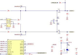
By consulting the gerber files provided on your site, I found the location of these components but it does not correspond to my board.
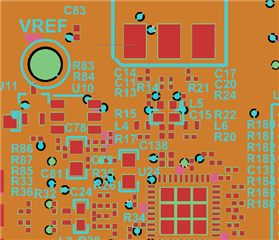
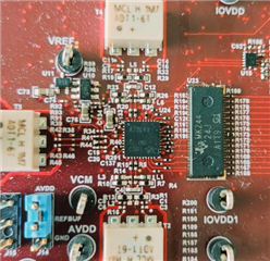
Is it possible to have the gerber files corresponding to the REV E version of the ADC3643 EVM to be sure of the components I need to solder and desolder?
Thanks
