This thread has been locked.

If you have a related question, please click the "Ask a related question" button in the top right corner. The newly created question will be automatically linked to this question.

ADS131M04-Q1: ADS131M04-Q1

Part Number: ADS131M04-Q1
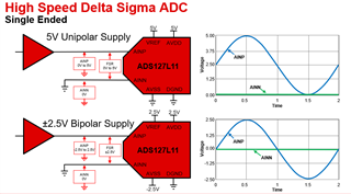
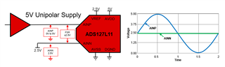
Other Parts Discussed in Thread: ADS127L18, ADS127L21, TINA-TI, ADS127L11

Tool/software:

Hello Ti,

I am looking for ADC which is capable of simultaneous sampling and operates at 3.3V, my highest frequency of interest is 15 kHz. Could TI suggest a suitable part?

ADS131M04-Q1 has maximum sampling rate of 64 KSPS, my question is it for every channel or since there are 4 channels it gets divided by 4 which is 16ksps available to each channel? Please let me know, as I have to finish off the part selection.

  • Hi Sumeet,

    if you are looking for an AEC-Q100 qualified solution, then ADS131M04-Q1 would be our best option currently for your requirements.
    The device includes four dedicated ADCs which are working in parallel. That means each ADC channel samples with up to 64kSPS.

    The one thing to note though is that the ADS131M04-Q1 uses a SINC3 digital filter. If you look at the digital filter frequency response in the datasheet (Figures 8-4 and 8-5), you will notice the attenuation of the input signal with increasing signal frequency.
    That means if you operate the device at 64kSPS, then your signals at 15kHz will get attenuated with ~3dB.

    If this attenuation is unacceptable, you could implement what we call a digital "droop-compensation filter" in your processor. This filter would then digitally correct for the attenuation of the SINC3 filter.

    In case you don't require AEC-Q100 qualification, then you should look at our ADS127L18 instead. This device offers the option of a "flat-passband" filter.

    Regards,
    Joachim Wuerker

  • Thank you, Joachim, for your informative reply, 

    I have one question regarding the interface of ADS127L18 with MCU, is that SPI or parallel, do you have any reference design and code for its interfacing with Arduino Uno.

    I have question whether AVDD should be 5 V, can I power it with 3.3V instead, and Do I need to have 1.8V for IOVDD? Please let me know. If I power, it with 3.3V, what will be maximum sampling rate that will be available? 

    In the datasheet there is mention of different mode with respect to voltage levels.

    Also I intend to use single ended operation.

  • Hi Sumeet,

    let me loop in my colleague who is a specialist for the ADS127L18 to get back to you.

    Regards,
    Joachim Wuerker

  • Hello Sumeet,

    We do not have any example code to interface to an MCU. 

    The ADS127L18 requires two interfaces.  SPI is only used to read and write to internal configuration registers.  You cannot read conversion results through the SPI port.  All conversion results are read over a separate data port interface, which uses Frame-sync (similar to the audio I2S interface).  The data port has options to use 1 to 8 DOUT pins for data, and also generates the data clock (DCLK) and the frame-sync clock (FSYNC).  Doing a quick search on the Arduino Uno, it looks like this MCU will not support frame-sync interface.

    AVDD can be powered from 3.3V, but your maximum data rate will be reduced to 200ksps for the wideband filter and 533ksps for the low-latency filters.  The IOVDD supply only supports 1.8V logic levels, with a allowed voltage range of 1.65V to 1.95V.

    If you would like to interface using only SPI, then I would suggest looking at the single channel ADS127L21; you can easily daisy-chain 4 devices over a single SPI port.

    Regards,
    Keith Nicholas
    Precision ADC Applications

  • Hello Keith and Jaochim,

    Thank you for your responses, I wonder is it possible for me to simulate the ADS response to my designed signal chain? I have attached my signal tina spice model to this message.

    6153.INA849 with JFE Front End With mic source impedancewithsingleendedsallenFilter - Copy.TSC

  • Hello Sumeet,

    You can use the ADS127L11 TINA-TI model with your attached signal chain.  This model will allow AC response simulation, noise simulation, as well as transient response (useful to verify if the input amplifier can properly drive the ADC inputs).

    https://www.ti.com/lit/tsc/sbam467

    The ADS127L11 Spice model only models the analog front-end; it does not model the digital features of the device.

    Regards,
    Keith

  • The ADC will be able to handle sinusoidal single ended inputs as well?

  • Hello Sumeet,

    Yes, the ADS127L18, ADS127L21, and ADS127L11 can handle single-ended inputs. Below are a few example configuration options.

    Regards,
    Keith

  • I need help with simulation,

    Can you provide me an email id where I can get tech support on my simulation model. Since this is part of our IP, I cannot attach my simulation model to this thread.

    Another question I have is for IOVDD voltage:

    What are pro and cons of using 1.8V versus 3.3V and 5 V for IOVDD.

    "Although the ADC provides flexible SPI clock options and the wide IOVDD voltage range, the following guidelines help achieve full data sheet performance. 1. If possible, use an SCLK signal that is phase coherent to the CLK signal (that is, ratios of 2:1, 1:1, 1:2, 1:4, and so on) 2. Minimize phase skew between SCLK and CLK (< 5ns) 3. Operate IOVDD at the lowest voltage possible to reduce digital noise coupling 4. If IOVDD ≥ 3.3V, consider operating SCLK continuously over the full conversion period to spread the effects of noise coupling over the full conversion period 5. Keep the trace capacitance of SDO/ DRDY ≤ 20pF to limit the peak currents associated with the digital code transitions"

    This tells that for reduced digital noise, IOVDD should be very low.

    Please revert me on my two queries. 

  • Hello Sumeet,

    The ADS127L18 only supports IO voltages up to 1.95V, so 1.8V typical.  The ADS127L11 and ADS127L21 support a wide IOVDD voltage from 1.65V up to 5.5V.  For lowest noise, it is best to use lower IO voltage levels, since digital activity will have some amount of coupling back into the ADC inputs.  Using standard clock ratios and minimum clock skew also help reduce noise coupling.  To be clear, this will have little impact on total SNR, but may degrade THD and SFDR.

    If you have any specific questions using the ADS127Lxx model, please ask them here.

    Regards,
    Keith

  • When I run the simulation model, I see instead of sine wave which is type of my input signal, the ADC output is a square wave, and I also get error like convergence problem and irregular circuit, since it is IP I cannot attach the simulation file to this thread. I will send you a message,

    Please correct me if I am wrong: If IOVDD is 1.8V then SPI bus will also be at 1.8V, and in such case I will need level translator to interface with MCU that runs on 3.3V or 5V DC.

  • Hello Sumeet,

    I responded to your simulation questions on the private chat.

    Yes, the ADS127L18 requires a 1.8V IOVDD supply, and the processor connected to it must either support 1.8V IO levels, or voltage level translators must be used.

    Regards,
    Keith