ADS1299: Not reading data from INx inputs

Part Number: ADS1299

Tool/software:

Hello,

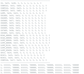
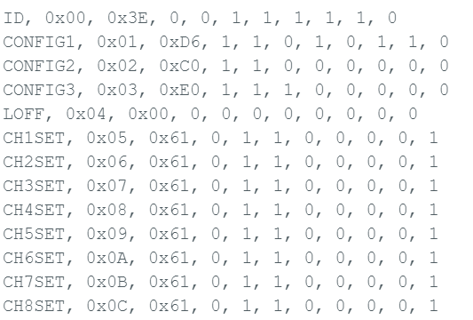
I am trying to read the data from de ADS1299 using an Arduino board. I have achieved the communication between Arduino and ADS1299, since I can read and write in the registers as it is show in this picture:

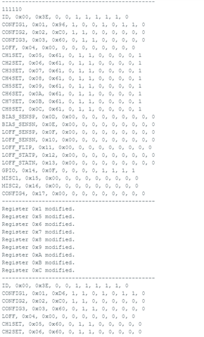
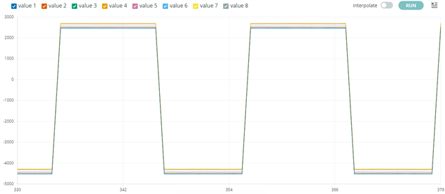
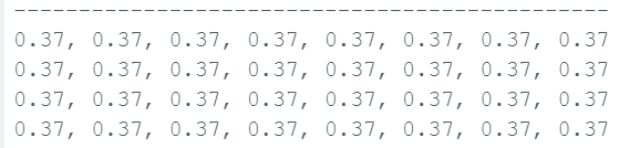
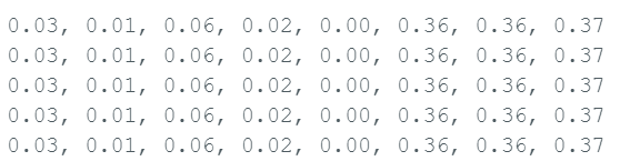
The problem comes when reading the data from the IN channels, it gives the following values all the time:


As I understand, the values that I am obtaining are related to the maximum values, like saturating. 

The code I am using in Arduino is the following:

#include <ADS1299.h>

ADS1299 ADS;

void setup() {
Serial.begin(115200);
delay(50);

//Pin 8 = RESET
pinMode(8, OUTPUT);
digitalWrite(8, LOW);
delay(50);
digitalWrite(8, HIGH);
delay(50);

ADS.setup(9, 10);
ADS.SDATAC();
ADS.getDeviceID(); //Funciton to return Device ID
//PRINT ALL REGISTERS... Read 0x17 addresses starting from address 0x00 (these numbers can be replaced by binary or integer values)
ADS.RREG(0x00, 0x17);
Serial.println("----------------------------------------------");

//Write register command (see Datasheet pg. 38 for more info about WREG)
ADS.WREG(CONFIG1, 0b11010110);
ADS.WREG(CH1SET, 0x60);
ADS.WREG(CH2SET, 0x60);
ADS.WREG(CH3SET, 0x60);
ADS.WREG(CH4SET, 0x60);
ADS.WREG(CH5SET, 0x60);
ADS.WREG(CH6SET, 0x60);
ADS.WREG(CH7SET, 0x60);
ADS.WREG(CH8SET, 0x60);
Serial.println("----------------------------------------------");

//Repeat PRINT ALL REGISTERS to verify that WREG changed the CONFIG1 register
ADS.RREG(0x00, 0x17);
Serial.println("----------------------------------------------");
delay(500);
ADS.START();
delay(10);
ADS.RDATAC();
delay(500);
delay(50);
}

void loop()
{
  ADS.updateData();
}
Any idea what is happening? 
Thanks
  • Hi Pablo,

    Thank you for your post. 

    It appears that you have configured all channels to use Gain = 6 V/V and normal electrode input (i.e. differential inputs connected to INxP and INxN pins). What voltages are applied to these pins during your measurements? If the pins are floating, it's possible for a differential offset voltage to develop, which exceeds the ADC positive or negative full-scale range when multiplied by the gain.

    If you're mainly interested in validating your code and SPI communication, you can reconfigure the register settings to short the PGA inputs internally and measure a near-zero offset voltage (with some noise), or you can measure the internal square wave or DC test signal options. This allows you to evaluate your data transmission and codes-to-volts conversion in your algorithm.

    Regards,

    Ryan

  • Hi Ryan,

    Thanks for your reply.

    I have checked the PGA configuration and I modified the CHnSET registers to 0x01 just in order to have a 1 V/V Gain and shorting the inputs but the data doesn't change:

    I am trying to read eeg signals, but shorting the inputs shouldn't be near to 0?

    I made the following changes in my code in order to obtain the previous registers:

    #include <ADS1299.h>

    ADS1299 ADS;

    void setup() {
    Serial.begin(115200);
    delay(50);

    //Pin 8 = RESET
    pinMode(8, OUTPUT);
    digitalWrite(8, LOW);
    delay(50);
    digitalWrite(8, HIGH);
    delay(50);
    ADS.setup(9, 10);
    delay(50);
    ADS.SDATAC();
    delay(50);
    ADS.getDeviceID(); //Funciton to return Device ID
    //PRINT ALL REGISTERS... Read 0x17 addresses starting from address 0x00 (these numbers can be replaced by binary or integer values)
    ADS.RREG(0x00, 0x17);
    Serial.println("----------------------------------------------");

    //Write register command (see Datasheet pg. 38 for more info about WREG)
    ADS.WREG(CONFIG1, 0b11010110);
    delay(15);
    ADS.WREG(CONFIG3, 0xE0);
    delay(15);
    ADS.WREG(CH1SET, 0b00000001);
    delay(15);
    ADS.WREG(CH2SET, 0b00000001);
    delay(15);
    ADS.WREG(CH3SET, 0b00000001);
    delay(15);
    ADS.WREG(CH4SET, 0b00000001);
    delay(15);
    ADS.WREG(CH5SET, 0b00000001);
    delay(15);
    ADS.WREG(CH6SET, 0b00000001);
    delay(15);
    ADS.WREG(CH7SET, 0b00000001);
    delay(15);
    ADS.WREG(CH8SET, 0b00000001);
    delay(15);
    Serial.println("----------------------------------------------");

    //Repeat PRINT ALL REGISTERS to verify that WREG changed the CONFIG1 register
    ADS.RREG(0x00, 0x17);
    Serial.println("----------------------------------------------");
    delay(500);
    ADS.START();
    delay(10);
    ADS.RDATAC();
    delay(50);
    }

    void loop()
    {
      ADS.updateData();
    }

    Any suggestion?
    Thanks in advance!

  • Hello Pablo,

    Yes, with input-short configuration and Gain = 1, the output codes should be very close to 0. It looks like your last function reads back the registers to confirm WREG was successful - everything looks correct?

    Can you probe the voltages on the following pins with respect to GND and let me know the result?

    • VREFP and VREFN
    • AVDD and AVSS
    • DVDD
    • VCAPx (x = 1 through 4)

    Regards,

    Ryan

  • Hi Ryan,

    I have checked the voltages that you mention, these are the followings:

    AVDD to GND = 2.501 V

    AVSS to GND = - 2.512 V

    DVDD to GND = 3.27 V

    VREFP to GND = - 2.5 V

    VREFN to GND = - 2.5 V

    VCAP1 to GND = - 1.31 V

    VCAP2 to GND = 0 V

    VCAP3 to GND = 3.9 V

    VCAP4 to GND = -2.5 V

    Do you see any mistake on the voltages?

    Thanks!! 

  • Hi Pablo,

    VREFP and VCAP4 (which is VREF/2) indicate that the internal reference is either not enabled or not working properly. This explains why the ADC output codes were saturated to ± full-scale. Are you issuing a reset pulse to the device nRESET pin after power up and before writing to any registers?

    Just to rule out any other issues, can you try leaving the internal reference disabled (nPD_REFBUF = 0b) and apply an external 2.4-V reference voltage to VREFP (note: 2.4 V is relative to AVSS, so -100 mV with respect to GND)? Then recapture the data with input-short configuration and check to see if the ADC output codes are near 0 as expected.

    Regards,

    Ryan

  • Hello Ryan,

    With regards to the Reset, I am following this sentence where I use the RESET pin before writing on the registers:

    void setup() {
    Serial.begin(115200);
    delay(50);

    //Pin 8 = RESET
    pinMode(8, OUTPUT);
    digitalWrite(8, LOW);
    delay(50);
    digitalWrite(8, HIGH);
    delay(50);

    ADS.setup(9, 10);
    ADS.SDATAC();
    ADS.getDeviceID(); //Function to return Device ID
    //PRINT ALL REGISTERS... Read 0x17 addresses starting from address 0x00 (these numbers can be replaced by binary or integer values)
    ADS.RREG(0x00, 0x17);
    Serial.println("----------------------------------------------");

    //Write register command (see Datasheet pg. 38 for more info about WREG)
    ADS.WREG(CONFIG1, 0b11010110);
    It is well done?
    On the other hand, since I did the hardware, I can not apply an external voltage in VREFP. Just to confirm, this would be the correct circuit for the VREF pins?


    My board was designed with the following VREF circuit, maybe the error is here:
    Regards,
    Pablo
  • Hi Pablo, 

    The first figure is correct - AVSS must connect to pin 25 (VREFN). If the board was manufactured according to the schematic in the second figure, you have shorted VREFP to the negative supply, and VREFN is floating at dc. This explains the behavior you're seeing.

    Maybe you can cut the trace between C22 and C21, and then short across C22 as a test?

    Regards,

    Ryan

  • Hi Ryan,

    After redesigning the PCB and correcting what we mention above about the VREF voltages, I obtain a VREFN = -2.5V and VREFP = +2V therefore I assume now that these references are working properly.

    However I have some doubts with respect to the VCAP voltages. Which are supposed to be the values of these? 

    I list you below the values I obtained with respect to GND (v+ on VCAP and v- on GND):

    VCAP1 = -1.3V

    VCAP2 = -16 mV

    VCAP3 = 4.4 V

    VCAP4 = -267 mV

    The values that I am using for the capacitors are these:

    Thanks again for your help!

    Regards,

    Pablo

  • Hi Ryan, 

    I would like to ask you too about two more points:

    1- I tried the test signal that you recommended and I obtain the following values from the 8 channels:

    I noticed that it appears a bit offset for every channel so I tried shortcircuiting the inputs as you mentioned and these are de values:

    these values are normal? the test signal seems to be working properly but I am not sure.

  • Hello Pablo,

    These VCAPx measurements all appear correct to me. They should be close to the following:

    • VCAP1 = Bandgap = AVSS + 1.2 V
    • VCAP2 = Vcm (mid supply) = (AVDD + AVSS) / 2
    • VCAP3 = charge pump = AVDD + 1.8 V
    • VCAP4 = AVSS + (VREFP - VREFN) / 2
  • The test signal results seem correct. Yes, each channel will still have a unique offset voltage, which can be calibrated by shorting the multiplexer inputs and recording the result. The amplitude of the AC test signal can be translated to volts assuming an LSB size of (2*VREF)/Gain.

    Regards,

    Ryan

  • Hello Ryan, 

    About the calibration, I'm having some doubts. First of all I tried to active the internal reference to check the dc offset voltage, which using the 1 LSB convertion gave me these values:

    I had these values for the registers:

    After recording the results as you mentioned, there is any way to calibrate the ads1299?

    On the other hand, I tried to avoid the internal reference to see the DC offset voltage:

    Before measuring EEG signals, I would like to ensure a 0 offset voltage, what would you recommend me to do?

    Thanks!

    Pablo