Other Parts Discussed in Thread: ADC12QJ1600-SP
Tool/software:
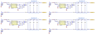
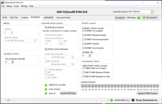
My team has set up a system using your ADC12QJ1600EVM connected to a Xilinx VCK190EVM board over the FMC bus to do sampling of 4 analog inputs at a 1.6Ghz rate. We have used your ADC12QJ1600EVMGUI SW to configure the board as shown in the screenshots below:
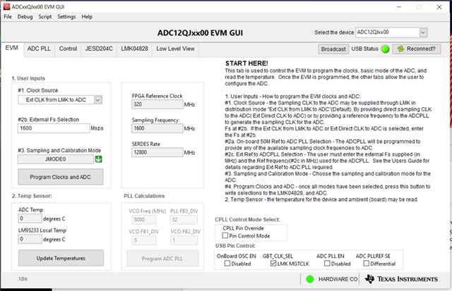
We are driving the LMK_CLK input to the board with an external signal generator at 1.6Ghz at 4dbm power level.
Notice that the ADC is in “Ramp test mode”. The 8 serial lanes go to a Xilinx Versal VCK190 board which includes a Xilinx xcvc1902-vsva2197-2MP-e-S FPGA configured with an 8-lane JESD204C decoder IP. The 256-bit output of the decoder is connected to a Xilinx ILA which shows the following sequence of data when the ADC board is running in “Ramp Test Mode”. This pattern repeats continuously. We believe this is correct. Please tell us if it is not.
0302010003020100030201000302010003020100030201000302010003020100
0706050407060504070605040706050407060504070605040706050407060504
0b0a09080b0a09080b0a09080b0a09080b0a09080b0a09080b0a09080b0a0908
0f0e0d0c0f0e0d0c0f0e0d0c0f0e0d0c0f0e0d0c0f0e0d0c0f0e0d0c0f0e0d0c
1312111013121110131211101312111013121110131211101312111013121110
1716151417161514171615141716151417161514171615141716151417161514
1b1a19181b1a19181b1a19181b1a19181b1a19181b1a19181b1a19181b1a1918
1f1e1d1c1f1e1d1c1f1e1d1c1f1e1d1c1f1e1d1c1f1e1d1c1f1e1d1c1f1e1d1c
2322212023222120232221202322212023222120232221202322212023222120
2726252427262524272625242726252427262524272625242726252427262524
2b2a29282b2a29282b2a29282b2a29282b2a29282b2a29282b2a29282b2a2928
2f2e2d2c2f2e2d2c2f2e2d2c2f2e2d2c2f2e2d2c2f2e2d2c2f2e2d2c2f2e2d2c
3332313033323130333231303332313033323130333231303332313033323130
3736353437363534373635343736353437363534373635343736353437363534
3b3a39383b3a39383b3a39383b3a39383b3a39383b3a39383b3a39383b3a3938
3f3e3d3c3f3e3d3c3f3e3d3c3f3e3d3c3f3e3d3c3f3e3d3c3f3e3d3c3f3e3d3c
4342414043424140434241404342414043424140434241404342414043424140
4746454447464544474645444746454447464544474645444746454447464544
4b4a49484b4a49484b4a49484b4a49484b4a49484b4a49484b4a49484b4a4948
4f4e4d4c4f4e4d4c4f4e4d4c4f4e4d4c4f4e4d4c4f4e4d4c4f4e4d4c4f4e4d4c
5352515053525150535251505352515053525150535251505352515053525150
5756555457565554575655545756555457565554575655545756555457565554
5b5a59585b5a59585b5a59585b5a59585b5a59585b5a59585b5a59585b5a5958
5f5e5d5c5f5e5d5c5f5e5d5c5f5e5d5c5f5e5d5c5f5e5d5c5f5e5d5c5f5e5d5c
6362616063626160636261606362616063626160636261606362616063626160
6766656467666564676665646766656467666564676665646766656467666564
6b6a69686b6a69686b6a69686b6a69686b6a69686b6a69686b6a69686b6a6968
6f6e6d6c6f6e6d6c6f6e6d6c6f6e6d6c6f6e6d6c6f6e6d6c6f6e6d6c6f6e6d6c
7372717073727170737271707372717073727170737271707372717073727170
7776757477767574777675747776757477767574777675747776757477767574
7b7a79787b7a79787b7a79787b7a79787b7a79787b7a79787b7a79787b7a7978
7f7e7d7c7f7e7d7c7f7e7d7c7f7e7d7c7f7e7d7c7f7e7d7c7f7e7d7c7f7e7d7c
8382818083828180838281808382818083828180838281808382818083828180
8786858487868584878685848786858487868584878685848786858487868584
8b8a89888b8a89888b8a89888b8a89888b8a89888b8a89888b8a89888b8a8988
8f8e8d8c8f8e8d8c8f8e8d8c8f8e8d8c8f8e8d8c8f8e8d8c8f8e8d8c8f8e8d8c
9392919093929190939291909392919093929190939291909392919093929190
9796959497969594979695949796959497969594979695949796959497969594
9b9a99989b9a99989b9a99989b9a99989b9a99989b9a99989b9a99989b9a9998
9f9e9d9c9f9e9d9c9f9e9d9c9f9e9d9c9f9e9d9c9f9e9d9c9f9e9d9c9f9e9d9c
a3a2a1a0a3a2a1a0a3a2a1a0a3a2a1a0a3a2a1a0a3a2a1a0a3a2a1a0a3a2a1a0
a7a6a5a4a7a6a5a4a7a6a5a4a7a6a5a4a7a6a5a4a7a6a5a4a7a6a5a4a7a6a5a4
abaaa9a8abaaa9a8abaaa9a8abaaa9a8abaaa9a8abaaa9a8abaaa9a8abaaa9a8
afaeadacafaeadacafaeadacafaeadacafaeadacafaeadacafaeadacafaeadac
b3b2b1b0b3b2b1b0b3b2b1b0b3b2b1b0b3b2b1b0b3b2b1b0b3b2b1b0b3b2b1b0
b7b6b5b4b7b6b5b4b7b6b5b4b7b6b5b4b7b6b5b4b7b6b5b4b7b6b5b4b7b6b5b4
bbbab9b8bbbab9b8bbbab9b8bbbab9b8bbbab9b8bbbab9b8bbbab9b8bbbab9b8
bfbebdbcbfbebdbcbfbebdbcbfbebdbcbfbebdbcbfbebdbcbfbebdbcbfbebdbc
c3c2c1c0c3c2c1c0c3c2c1c0c3c2c1c0c3c2c1c0c3c2c1c0c3c2c1c0c3c2c1c0
c7c6c5c4c7c6c5c4c7c6c5c4c7c6c5c4c7c6c5c4c7c6c5c4c7c6c5c4c7c6c5c4
cbcac9c8cbcac9c8cbcac9c8cbcac9c8cbcac9c8cbcac9c8cbcac9c8cbcac9c8
cfcecdcccfcecdcccfcecdcccfcecdcccfcecdcccfcecdcccfcecdcccfcecdcc
d3d2d1d0d3d2d1d0d3d2d1d0d3d2d1d0d3d2d1d0d3d2d1d0d3d2d1d0d3d2d1d0
d7d6d5d4d7d6d5d4d7d6d5d4d7d6d5d4d7d6d5d4d7d6d5d4d7d6d5d4d7d6d5d4
dbdad9d8dbdad9d8dbdad9d8dbdad9d8dbdad9d8dbdad9d8dbdad9d8dbdad9d8
dfdedddcdfdedddcdfdedddcdfdedddcdfdedddcdfdedddcdfdedddcdfdedddc
e3e2e1e0e3e2e1e0e3e2e1e0e3e2e1e0e3e2e1e0e3e2e1e0e3e2e1e0e3e2e1e0
e7e6e5e4e7e6e5e4e7e6e5e4e7e6e5e4e7e6e5e4e7e6e5e4e7e6e5e4e7e6e5e4
ebeae9e8ebeae9e8ebeae9e8ebeae9e8ebeae9e8ebeae9e8ebeae9e8ebeae9e8
efeeedecefeeedecefeeedecefeeedecefeeedecefeeedecefeeedecefeeedec
f3f2f1f0f3f2f1f0f3f2f1f0f3f2f1f0f3f2f1f0f3f2f1f0f3f2f1f0f3f2f1f0
f7f6f5f4f7f6f5f4f7f6f5f4f7f6f5f4f7f6f5f4f7f6f5f4f7f6f5f4f7f6f5f4
fbfaf9f8fbfaf9f8fbfaf9f8fbfaf9f8fbfaf9f8fbfaf9f8fbfaf9f8fbfaf9f8
fffefdfcfffefdfcfffefdfcfffefdfcfffefdfcfffefdfcfffefdfcfffefdfc
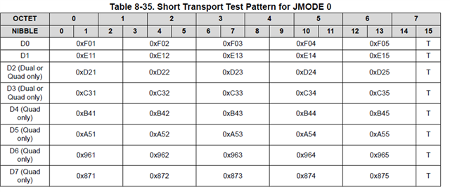
After we got the above working, we switched the test pattern on the board to “Transport Test Mode”. According to the adc12qj1600-sp.pdf datasheet we should see the following pattern coming from the JESD decoder.
Unfortunately, we see nothing similar to the above. The following is the pattern we see at the output of the JESD204C decoder. The pattern repeats continuously.
87721887a5521aa5b4421bb496621996f0021ff0e1121ee1c3321cc3d2221dd2
5087743850a5543a50b4443b5096643950f0043f50e1143e50c3343c50d2243d
According to the datasheet the tail “T” bits should be 0’s. We see nothing in the above pattern which looks like 0’s every 64-bits, not are patterns similar to the expected patterns shown in the datasheet figure.
We are getting a 320Mhz reference clock in the FPGA as verified with the IBERT circuitry. We have run PRBS31 checks in the FPGA using the PRBS31 generator in the ADC and they check without errors. rx_tvalid is 1 at the output of the JSED204C decoder, which indicates that the decoder thinks it is receiving valid data. Multiframes are 16 frames long, as they should be. We are driving the SYNCSE input of the ADC with the rx_sync output of the JESD204C IP as recommended by Xilinx. When the JESD204C IP is reset the rx_sync output activates and the JESD204C system goes through its resynchronization process as it should.
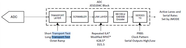
According to the following figure from the ADC datasheet the “Octet Ramp” test and the “Transport test” enter the JESD204C block at the same place, the two tests simply generate different data to be sent out over the JESD204C link. It would appear to us that if the “Ramp Test” works then the “Transport Test” ought to work since the ramp data and the transport data are both going through exactly the same circuitry going to the serial outputs of the ADC, and the same circuitry in the FPGA from the serial inputs to the outputs of the JESD204C decoder.
Is there anything else that may be wrong in our design that may be causing this problem. Is it possible that we simply have a defective ADC board?
Additionally, we have done something very similar with the ADC12DJ5200EVM board operating in JMODE30, and it appears to work fine. We can see the transport data that is expected. Of course, this was with a different FPGA design since JMODE 30 uses 64B/66B encoding where JMODE0 uses 8B/10B encoding.
Thanks for your assistance.
Terry Coleman