ADC12QJ1600EVM: GUI Configuration

Part Number: ADC12QJ1600EVM
Other Parts Discussed in Thread: TI-JESD204-IP, ADC12QJ1600

Tool/software:

Hello,

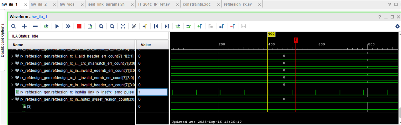
I am working with the ADC12QJ1600 EVM and the TI-JESD204-IP and have questions on how to configure the ADC12QJ1600 EVM GUI. I have set up the JESD IP to be 64b/66b, receiving with 4 lanes and believe with an external clock connected to LMK CLK, I can pass patterns to my FPGA that should be viewable on the ILA.

I believe my constraints are correct (FPGA_GBTCLK0_FMC from ADC mapped to refclk in the IP, FPGA_SYSREF_FMC to sysref and FPGA_CLK_FMC to sys_clk, and the data lanes).

I am using JMODE8 with 833MHz external clock to start with, as this results in a lane rate and FPGA clk similar to what is default in the JESD-IP as I just wanted to see any signal come through, and changed the JTEST register to attempt ramp and transport test modes but could not see any results in the FPGA ILA.

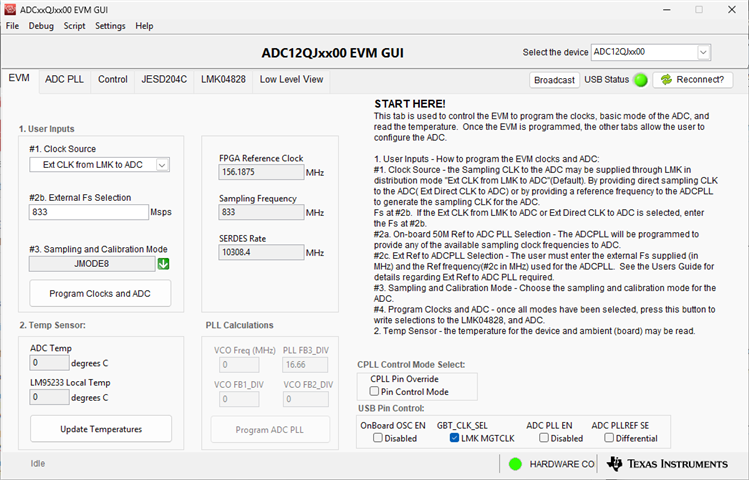
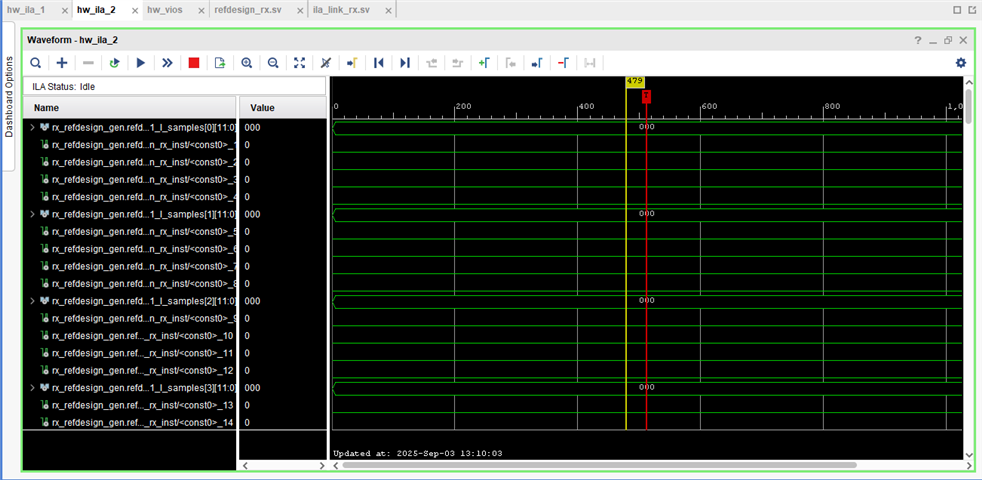
I would like if someone could run me through the settings I need to change to make the ADC compatible with the IP, to make signals visible in the ILA, so I can confirm that the ADC, and hence the JESD IP are set up correctly.

Thank you.

  • Hi Aaron,

    Kindly let us know which FPGA you are trying to target. The TI JESD IP archive contains a number of reference designs that can be used as starting points based on the target FPGAs. However, the selected reference design needs to be edited to make its JESD parameters match that of the ADC in JMODE8. This includes the following:
    1> Editing the jesd_link_params.vh file 
    2> Customizing the transceiver (xci) file through the transceiver wizard to match the lane rate and reference clock settings (based on what the EVM provides to the FPGA)
    3> Editing the refdesign_rx.sv file to map the lane data to samples. This depends on the JMODE mapping between lane/sample data, as illustrated in the datasheet.

    The user guide for the IP explains the various parameters as well as the lane/sample mapping procedure. 

    Kindly let us know how we can help further.

    Regards,
    Ameet

  • Hi Ameet, 

    I am doing testing with the ZCU102 64b/66b ref design. I believe I have already done most of the necessary modifications for my 4 lane receiver setup. Besides setting constraints I have:

    > edited the ADC resolution, number of tx/rx lanes, quads, lane mapping and polarity in the jesd_link_params.vh file

    > left the transceiver xci file as default besides reducing the number of channels to 4 (leaving line rate at 10.3125 Gb/s and 156.25 MHz Free running and DRP clock frequency) and configuring the ADC GUI to match this as close as I could, as I assumed the line rate and clock did not have to match perfectly to see an output from ADC

    I was not aware that I had to edit refdesign_rx.sv file, my only change here was commenting out the following code as I thought this was creating errors due to the change to 4 lanes:

    /*
    assign ch3_I_samples[i] = rx_lane_data[4][63-16*i -: ADC_RES];
    assign ch3_Q_samples[i] = rx_lane_data[5][63-16*i -: ADC_RES];
    assign ch4_I_samples[i] = rx_lane_data[6][63-16*i -: ADC_RES];
    assign ch4_Q_samples[i] = rx_lane_data[7][63-16*i -: ADC_RES];
    */

    Regardless, my main aim was just to see some signals in the ILA while passing patterns from the ADC so I can debug from there, and to get guidance on how to configure the ADC GUI, as I thought that my current design would be able to see some of the patterns, even if they were not mapped correctly.

    I am not sure if the problems are stemming from the way I configured the ADC or my FPGA design, so would it be possible to be provided with the list of necessary changes I would need to make in the ADC GUI for my application to confirm that the ADC is operational?

    Thank you.

  • Hi  ,

    Update, I have since followed the 8.3 Initialization Set Up steps in the ADC12xJ1600 datasheet and then set the pattern mode. Yet in the ILA aside from the rx_sync_n signal which is always 1, I can only see rx_lemc_pulse pulses, as below.

    All other values, including from the data lanes, return as 0s. Any idea why this might be? Thank you.

  • Hi  

    I also made a copy of the project and did simulation loopback following steps here:

     https://e2e.ti.com/support/data-converters-group/data-converters/f/data-converters-forum/1230925/ti-jesd204-ip-simulation-of-loopback-design-in-vivado 

    It all worked as expected, so I believe the FPGA design is fine? However, the equivalent Rx only project design does not see any data (only the lemc pulses) after I program the FPGA and configure the ADC. I double checked that the lane rates and FPGA reference clock match between the FPGA and the ADC.

    I have tried initializing the ADC in the GUI following the steps in chapter 3 of the ADCxxQJxx00 Evaluation Module User's Guide and also with the low level view following section 8.3 of the ADC12QJ1600 datasheet. 

    But rx lane data valid does not go high and so I do not see any of the adc patterns. I would appreciate any advice on how to solve this, thank you.