


Hi all,
I'm going to use TLC5540 with PIC18F4550 microcontroller.
Do I need 74AC573 IC when interfacing microcontroller and ADC .
(I'm referring the application note "Interfacing the TLC5540 Analog to Digital Converter to the TMS320C203-80 DSP (APPLICATION REPORT: SLAA032)".)
for my design ???
My microcontroller can handle 5v signals. Im hope ur kind quick response.
regards
sampath


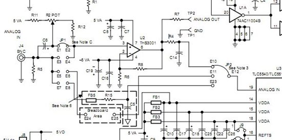
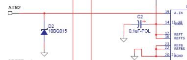
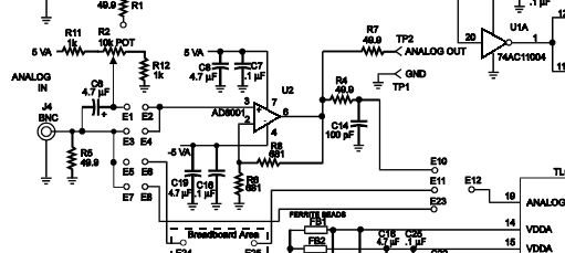
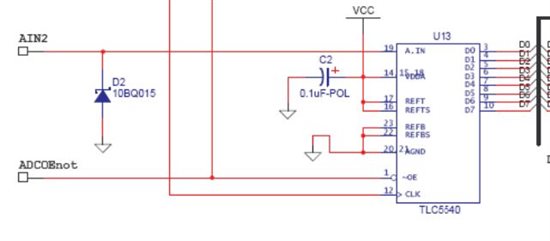 figure 1
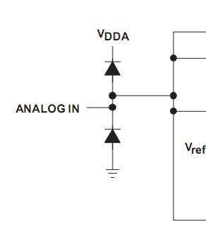 figure 2