This thread has been locked.
If you have a related question, please click the "Ask a related question" button in the top right corner. The newly created question will be automatically linked to this question.
Hi,
First of all, I'm a computer scientist with no electrical engineering background so I'm likely to make mistakes in my design and reasoning.
I have the same problem as Eran. The measurement error depends on Rbias, a precision resistor costs as much as the ADS1248 and it introduces another error. I used the following schema to measure an RTD without using Rbias.
Internal reference 2.048V, IDAC set to 1.5mA , PT1000 RT, PGA=1
I tested this with a 1KOhm 1% resistor and it seems to work well.
1K Ohm (0˚C) corresponds to a reading of 1.5V, max would be 1365Ohm (91˚C).
I took 1000 samples and they got a st dev of 0.02 Ohm or 0.005˚C.
I'd like to improve on this but don't really know how. I think the main problem is that I don't use the full range available, only 1.5-2.048V and that I can't use the PGA in this configuration.
All comments and ideas are very welcome!
best regards,
Beau
Hello Beau,
When using the ADS1248 to measure an RTD using the programmable IDAC current sources; it is recommended to configure the device in a ratiometric configuration. Also the user needs to consider the input voltage range requirements of the device (common-mode voltage requirements)
The RBIAS resistor has two functions:
1) The IDAC current flows through the RBIAS resistor, generating the Reference voltage used for conversion. Since the IDAC current is used both as an excitation source for the RTD and also to generate the reference voltage, this configuration creates a ratiometric measurement. The drift and noise of the excitation IDAC source is seen both at the input signal path and at the reference signal path; therefore the errors due to drift and some of the noise of the excitation tend to cancel. This makes a strong case for using the RBIAS resistor.
2) The RBIAS resistor biases the RTD at the optimal common-mode voltage at the middle of the supplies. Please keep in mind that the ADS1248 has a common-mode voltage requirement where both inputs INP and INN should be at least 0.1V away from both the AVSS and AVDD analog supply rails. Depending on the magnitude of the differential signal applied accross the inputs, and the PGA gain setting, the inputs may require more than 0.1V voltage headroom.
Please find below the application note showing the ADS1248 performing RTD measurements:
http://www.ti.com/lit/an/sbaa180/sbaa180.pdf
Also below is a design note that explains the ADS124X and ADS114x common-mode voltage requirements in more detail:
Best Regards,
Luis
Hi Lius,
Thanks for the fast reply.
Doesn't your first point for using Rbias, noise cancelling/ratiometric configuration, also hold when using the internal reference?
The internal reference is used to generate the IDAC currents and therefore the errors due to drift and some of the noise tends to cancel? In the end, everything is based on the internal reference. Internal ref->IDAC->external ref using Rbias. It's not clear to me how the extra IDAC/Rbias step improves noise performance.
How about using Rbias to solve the cmi voltage problem but use the internal reference? This would allow using a cheaper Rbias resistor with a bigger tolerance.
cheers,
Beau
Hi Beau,
On your first question, there will be some ratiometric cancellation using the internal voltage reference for conversion and the IDAC for excitation; since the bandgap reference circuit is used to bias the current source banks to generate the programmable current sources. Therefore, there will be a good amount of correlation between the drift and some of the noise that is present on the voltage reference and the drift/noise present on the IDAC.
However, when using the programmable IDAC to excite the RTD and also to produce the voltage reference through RBIAS, since you are using exactly the same circuit to excite the RTD and to generate the reference voltage, there will be closer correlation of the noise/drift present on the signal path and the reference path; therefore a more effective ratiometric cancellation.
In the circuit above, you have the negative input of the ADS1248 directly connected to AVSS; which will put the device outside the allowed common-mode voltage range. The easiest thing to do is to place a resistor in series with the RTD between AVSS and the ADS1248 negative input, and in this manner, the negative input will have some headroom above the negative supply rail.
Best Regards,
Luis
Hello Luis,
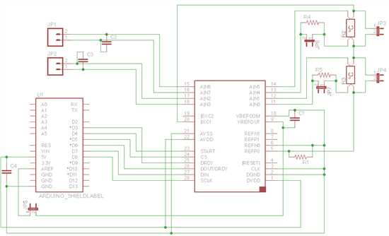
I drew a schematic design for ADC thermocouple/RTD shield for the arduino. Could you have a look and see if it looks ok / can make some improvement suggestions?
The jumpers would allow me to switch between 3-wire hardware R comp and 4 wire setup (JP6/7) and to disconnect the RTD's (JP3/4).
Thanks!
Beau
Hi Beau,
Below are some suggestions:
-- RESET Pin Connection: The RESET pin needs to be pulled high for the device to operate. You may consider using a I/O from the microcontroller to control the RESET pin. At minimum, you will need a pull up resistor to the DVDD supply (100kOhm)
-- Supply Bypass Capacitors: The bypass capacitors at the supply pins AVDD and DVDD are very important. It is recommended to have separate bypass capacitors (at least 0.1uF) for the Analog and Digital supplies. The capacitors must be in close proximity to the supply pins on the board layout. Please refer to the ADS1248EVM schematic for an example. It is also important to ensure that the voltage supplies used are low noise stable supplies. In applications where a switching supply or switching regulator is used to generate the voltage supplies, a low-noise Linear regulator with high PSRR is placed in front of the switcher to eliminate/attenuate the ripple.
-- Board Layout and Ground Plane: The ADS1248 is a 24 bit converter; the board layout and grounding scheme is also as critical as the schematic and components used to obtain the desired performance. It is important to plan ahead about the routing of the signals and grounding scheme to be used. Please see a link below for general information regarding board layout considerations when working with Analog to Digital converters. Ensure the VREFCOM pin and VREFN have a low short (low inductance) connection to the analog ground plane. Ensure to route the analog sensitive signals (and their return path) away from the digital signals and noise sources.
http://e2e.ti.com/support/data_converters/precision_data_converters/w/design_notes/general-pcb-layout-questions.aspx
-- Cold Junction Compensation (Thermocouple Measurement): In order to perform a high precision thermocouple measurement, the user needs to account for the changes of temperature that occur on the cold junction (thermocouple connector) and perform cold junction compensation. When using the ADS1248; this is typically performed using an external precision temperature sensor (such as the TMP112) or an RTD. An example is shown on the application note below on page 5, under thermocouple application with RTD cold junction compensation;
http://www.ti.com/lit/an/sbaa180/sbaa180.pdf
There is also a link below to an application note regarding a different device (ADS1118); but many of the concepts regarding the cold junction compensation are explained in good detail.
http://www.ti.com/lit/an/sbaa189/sbaa189.pdf
-- RC Low Pass Filter for the Thermocouple measurement: Consider adding series resistors to the thermocouple channels for the low pass anti aliasing filter. Attached is a slide of the typical configuration recommended for a low-pass filter using a differential capacitor and 2 common-mode capacitors. The differential capacitor is typically 10x larger in magnitude than the common-mode capacitors. (Please refer to attachment for more detail).
6253.lowpassdiff.ppt
-- 3-Wire/4-wire RTD connections: If I interpreted the schematic correctly, R2, R3 are two RTD's that could configured on the 3-Wire configuration or the 4-Wire configuration. You probably need to connect the bottom (negative connection) of R2 (RTD) to VREFP0. The top or positive connection of R3 (RTD) should be connected to the IEXC2. Attached are examples of RTD connections using the 3-Wire and 4-wire configuration that may be helpful.
8640.forum.pdf.
On the board layout, the 3-Wire RTD configuration is sensitive to impedance mismatches on the board/traces connecting the positive and negative connections to the RTD. For example, the series resistance on the path connecting the RTD to AIN0 and AIN1 must be carefully matched on the board layout.
-- The bias resistor R1 produces the reference voltage as a function of the excitation current. This produces a ratiometric measurement since the noise and drift of the excitation is seen both at the reference path and the signal path. The idea of the ratiometric measurement is that the same noise signal is seen both at the signal and reference path. There is usually a trade-off that occurs between adding external low pass filters and how well the ratiometric cancellation works. In some applications where there is high frequency RF noise present , an RF low-pass filter could be beneficial; where the ratiometric configuration still cancels the excitation low frequency noise and drift and the RC filter eliminates the RF high frequency noise. Depending on the noise present in the environment, filtering may be beneficial on the ratiometric RTD measurement (you may need to experiment). On the board design, you may consider having a footprint for an optional capacitor across VREFP and VREFN and maybe other footprints for optional filters across the inputs of the device where the RTD measurement takes place for added flexibility.
Thank you and Best Regards,
Luis
Hi Luis,
Thanks for all the feedback.
I have a few more questions:
Luis Chioye said:-- 3-Wire/4-wire RTD connections: If I interpreted the schematic correctly, R2, R3 are two RTD's that could configured on the 3-Wire configuration or the 4-Wire configuration. You probably need to connect the bottom (negative connection) of R2 (RTD) to VREFP0. The top or positive connection of R3 (RTD) should be connected to the IEXC2.
What would be the problem with using only one IEXC running through all attached RTDs?
Can the filter on the thermocouple also be used on the RTD measurment?
Is there any advantage to using a bipolar supply?
Thanks!
Beau
Hi Beau,
--> It is possible to run one IDAC current through both RTDs in your design; but you will need to verify that enough headroom is given for the (2) RTD's under all temperature conditions. The IDAC current has a voltage compliance, and in addition, the ADS1248 has a common-mode voltage range requirement that depends on the PGA Gain used, Analog Voltage supplies and the differential voltage. The recommended configuration with only (1) RTD in the path may allow for more flexibility/headroom to allow a larger Reference voltage and therefore a higher PGA Gain.
The IDAC excitation source current voltage compliance spec is shown in Figure 47 page 22.
The following links provide a detail explanation of the common-mode voltage requirements of the device; also there is another post with an example that could be helpfult where the common-mode voltage range requirements are calculated for a 3-Wire configuration for hardware compensation on your design.
Common-mode Design Notes
http://e2e.ti.com/support/data_converters/precision_data_converters/w/design_notes/1370.input-voltage-range-requirements-for-the-ads1248-and-ads1148-families.aspx
3-Wire RTD common-mode/differential mode calculation example
http://e2e.ti.com/support/data_converters/precision_data_converters/f/73/p/193943/693044.aspx#693044
--> The chosen filter will depend on the RTD configuation used and the noise present in the application environment.
When using the 4-wire configuration, you may use a filter similar to the one provided on the thermocouple. There is usually a trade-off that occurs between adding external low pass filters and how well the ratiometric cancellation works. On applications where there is high frequency RF noise present or where the RTD sensor wires could pick up RF noise, a high frequency corner low-pass filter on the 10's kHz could prove to be beneficial; where the ratiometric configuration still cancels the excitation low frequency noise and drift and the RC filter eliminates the RF high frequency noise. Other users working on very noisy environments prefer to use even lower frequency low -pass filters and in some situations this provides the best result due to their noise environment.
When using the 3-Wire configuration, the IDAC current flows through the INN and INP lines connected to the RTD. In this case, current will flow through the low-pass filter resistors. Since the 3-wire configuration requires the RTD positive and negative connections to be carefully matched; any mismatch of the RC filter resistors will cause errors; therefore, the filter resistors will need to be precision or closely matched. In addition, in the 3-Wire with Hardware compensation (with RCOMP), the RCOMP resistor may produce a mismatch on the corner frequency seen by the ADS1248 positive and negative inputs; perhaps placing the RC filter before the RCOMP resistor may mitigate this effect. Some users configure the RTD without filtering and rely in the ratiometric configuration without filtering; or only use a capacitor across the reference inputs. Some experimentation may be required depending on your application.
6811.3wire_filter.pdf
--> In applications where the measured thermocouple is grounded and not floating with respect to the AVDD/AVSS analog supplies; bipolar supplies are required to keep the thermocouple in the allowed common-mode voltage range close to the middle of the supplies, If you decide to use bipolar AVDD/AVSS +/-2.5V supplies, ensure VREFN is connected to AVSS...
Best Regards,
Luis