


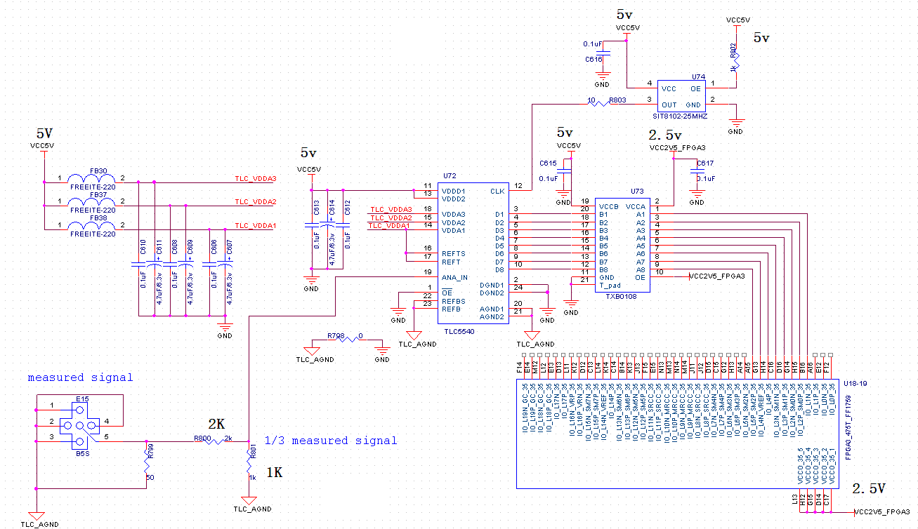
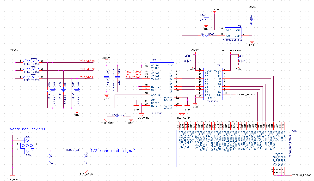
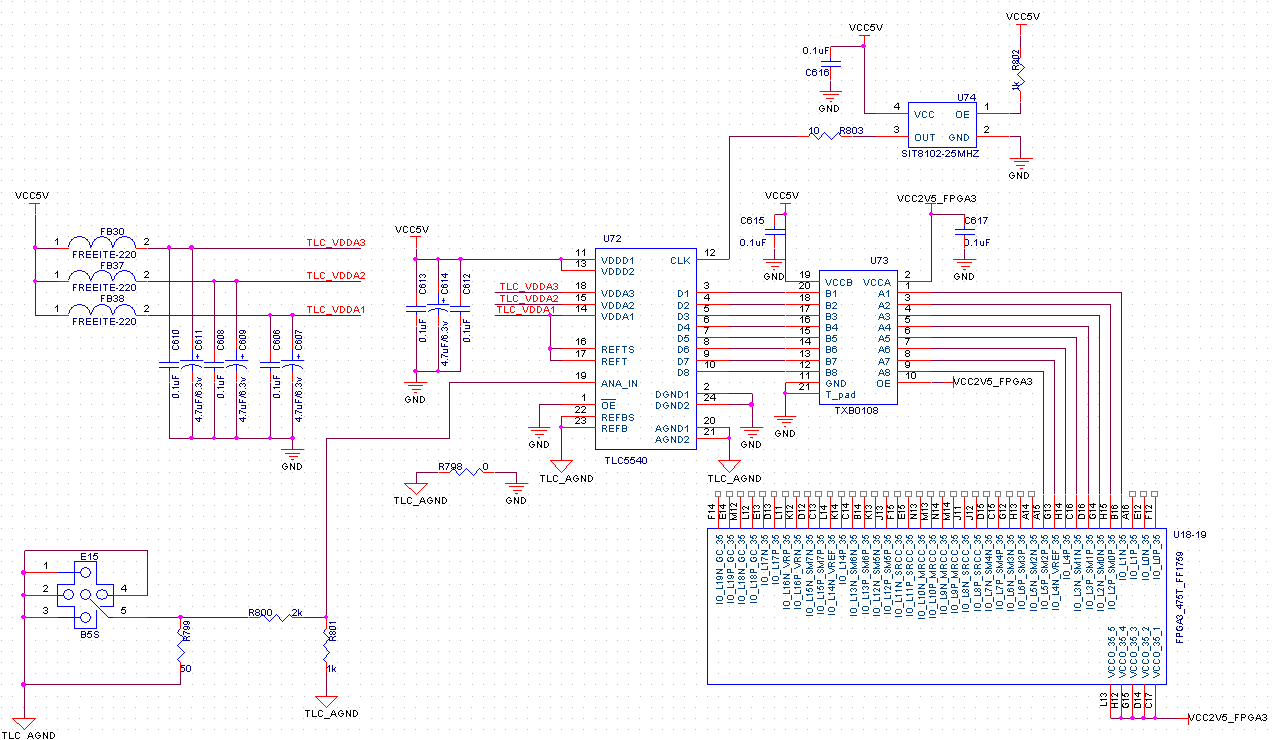
From the datasheet of the TLC5540.
I have some questions i can not sure.
1.If i want the chip of TLC5540 can operate with Vreft - Vrefb = 5 V ,i connect the pins "REFBS" and "REFB" to the GND, and connect the pins "REFTS" and "REFT" to the +5V. Is it right ?
2.Can the measured analog signal be durectly connected the analog input port (pin19) ?
3.What is the input clock's level ? Is it 5v ?
4.What is the outputs' (D1--D8) level ? Is it 5v ? If i want to connect the output of TLC5540 to the virtex6 FPGA , but the maximum voltage virtex6 FPGA can accept is 2.5v , i use a level converter (5v to 2.5v) ,for example TXB0108 . Is it ok ?
5.What is the vaule of the input impedance of the chip ? Because I want to divide the measured signal ,then connect the dividen siganl to the analog input port (pin19),I need to know the value of the input impedance of the chip!
Followed is the schematic :

