This thread has been locked.

If you have a related question, please click the "Ask a related question" button in the top right corner. The newly created question will be automatically linked to this question.

DAC7821 Positive Voltage Supply

Other Parts Discussed in Thread: OPA227, OPA277, REF5025, DAC7821, LMH6640, ADS1605, THS4502, THS4503

I am planning to use the circuit provided in the application section to provide positive voltage supply (Figure 28 in the datasheet). Regarding this circuit I have a couple of questions. Firstly, for the -2.5V reference is it coming via the inverting connection of the first OPA227? And for achieving this what supply should be provided for this opamp? Secondly, could someone list a good recommendation for the voltage reference? I am having a hard time searching for the information about the power consumption for both the DAC and opamp. Thanks in advance. 

  • Hi Junheng,

    The reference device generates  a positive 2.5V reference from GND. The negative reference is created by the level shifting of the reference. Since the output of the reference is forced to a virtual ground through the OpAmp, the only way for the reference to cope with this is to drop its GND pin to negative 2.5V.

    As for the power supplies used for the OPA, the datasheet of the OPA277 suggests using (+/-) 5V for the supplies, which should be sufficient for your application.

    The ideal reference would most likely be the REF5025, but you can probably get away with the REF5025A.

    The DAC7821 lists its current consumption to a max of 5uA.

    The OPA277 lists its current consumption to a max of 825uA per amplifier.

    Keep in mind that these current consumptions are for the devices alone. When they are loaded or generating current these will be added to the demand of your supplies.

  • Thank Eugenio for your response. In fact, I have another problem about this configuration of generating positive voltage supply. There is a capacitor C1 that is connected between the voltage output node and the Iout1. I am assuming it is acting to feedback but I hope you could give me more information about the funciton of the capacitor and how to decide its value exactly. 

  • C1, the compensation capacitor that you mention, is recommended in order to minimize stability issues. These issues generally come from the parasitic capacitive between the leads of the OpAmp.  The compensation capacitor, is aimed to reducing the amount of ringing seen at the output of the OpAmp. The calculation for this compensation capacitor is fairly involved. In this case, a simplistic rule would be: The larger your parasitic cap load, the larger your compensation capacitor should be.

    If you wish to calculate this exactly, you may want to take a look at this document.

    http://www.ti.com/lit/an/sloa020a/sloa020a.pdf Look at part 7 Lead compensation.

    This document goes into detail as to how to calculate the compensation capacitor.

    If cap load stability is a concern in your application, using an OpAmp with larger GBW and larger capacitive load than the OPA277 will be ideal. The datasheet of the OPA277 shows a graph on page 8 that displays the amount of overshoot across different capacitive loads.

    In order to help you some more with this issue I would need to know what capacitive load you would be expecting.

    #EDIT

    If you will be driving a large capacitance you may also need to look into some other compensation schemes.

  • For my design, I will need to connect the output in the positive voltage configuration to the amplifier LMH6640. Other capacitive loads will be some bypass capacitors. What do you think compensating capacitor will be appropriate for this circuit?

  • Besides the question above, for my circuit I need to handle both high frequency and low frequency signals. And I am using both DAC7821 and ADS1605. Thus I am wondering what the frequency responses for them look like? In particular, whether the frequency response still has a rather flat frequency response at DC?

    Another question is specifically about the positive supply circuit listed as Fig 28 in the datasheet for DAC7821. What bypassing capacitors do you recommend for this circuit (value and number)? 

    I really appreciate your help and thank you in advance!

  • Hi Junheng,


    Unless you expect a lot of parasitic capacitance on the pins of your OpAmp a 3pF compensation cap should be enough.


    You can observe parasitic capacitance from:

    • Long traces
    • Traces that are close to each other.
    • Ground and power planes.


    So inherently the recommendations would be, keep input leads as short as possible. Try to maintain other leads away from input leads, specially the inverting input pin. And finally, try to apply pour cut-outs for any planes going above or below the inverting input pin, meaning that no planes should be directly under or above the inverting lead of the OpAmp. If you expect to see inevitable parasitics, use a 5pF cap to stabilize the output.

    Both devices perform really well at DC. What your your high frequency of interest?

  • Hi Eugenio,

    I want to ask something more about the frequency responses of the two chips. It is good to know that they work really well at DC, would their frequency response be rather flat near the DC as well? We are expecting to operate at 2 MSPS for both so it would be nice if the frequency response maintains as flat for this range. Also, about the driver circuit provided in the Figure 11 in the datasheet for ADS1605, would the frequency response remain as flat (shown in Figure 19) if we are using this configuration?

  • Junheng,

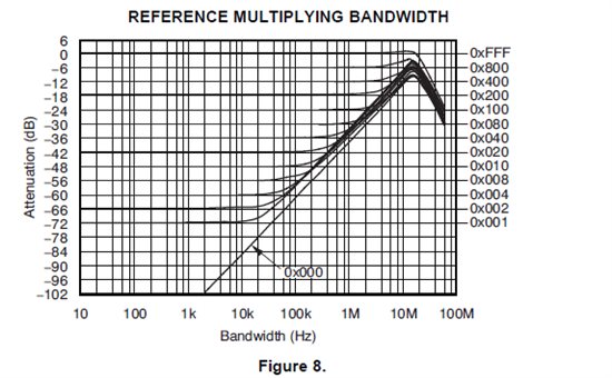
    I'm not very clear on what your application of these two devices will look like. Can you share a schematic or specific design goals? Are you using the DAC7821 in an attenuator application? (i.e. a signal applied at the reference input that is attenuated at the DAC output?). If that's the case, the DAC7821 does not include any output buffer circuitry on silicon, as is typical of multiplying DACs. The device is simply a digital interface and a trimmed R-2R ladder structure. With that in mind, there is nothing in place to purposely limit the bandwidth of the device, but parasitics on silicon will limit the device's bandwidth. This performance is summarized by Figure 8 in the datasheet and is inserted below:

    As you can see from the plot, the devices performance as an attenuator radically changes over frequency, and at very high frequency it does not serve very well as an attenuator. 

    If your interest is in using the DAC7821 to generate ac signals at 2MHz it certainly has bandwidth to create this signal but your precise requirements in terms of SNR, THD, and SFDR may require a DAC with a higher data rate. Additionally, you called out the OPA277 earlier in this thread - I'm not sure if you intended on using this device or not - but it's unity gain bandwidth is at 1MHz so you will not have good success using the OPA277 in this system.

    Regarding the ADC in this system, generally speaking a delta-sigma ADC does have a very flat frequency response at near DC. As frequency increases the  response will remain relatively flat but there will of course be some roll off, it really depends on the filter architecture and I don't have any information on hand to describe what sort of digital filter is implemented with this device. There is some useful data in the typical characteristics section of the ADS1605 datasheet, though, that show pretty good SNR, THD, and SFDR results with FIN of 2MHz. I do not support delta-sigma ADCs so it may be beneficial for you to post another thread requesting more information about the frequency response of the ADS1605.

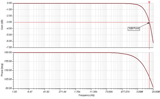
    The recommended circuit driving the input in Figure 11, the THS4502 is a very wide bandwidth differential amplifier with a unity gain bandwidth of 370MHz, the application circuit itself has a 3dB cutoff at approximately 12.45MHz. See below:

     I hope this helps.

  • Hi Kevin,

    Thank you for your detailed response. Based on your description, I think I am fine about the ADC part. Regarding the DAC part, I have another problem that I would like to ask you about. Since I am going to use the circuit provided in Figure 28 from the DAC7821 datasheet, I am wondering if you could tell me more about the bypassing capacitors for the circuit, for both DAC and OPA277.

    Thanks,

    Junheng

  • Hello Junheng,

    I apologize for forgetting to cover your query about the bypass capacitors in my previous post. In general I like to use a parallel combination of a 100pF and 0.1uF capacitors on any analog supply rail. For digital supply rails I just use a single 0.1uF capacitor. The parallel combination is useful because it helps to overcome the performance of real capacitors that exhibit self-resonance properties that may allow for very high-frequency components to sneak into the analog supplies. This is still possible using the parallel combination but it widens the stop-band on sensitive analog supplies. It may be considered over-kill to use this parallel combination and should not be considered necessary, but 0.1uF should be included on all supplies at least.

  • Hi Kevin,

    I have nother following question for you. In the Figure 11, where should V_CM be connected? 

  • Junheng,

    Figure 11 of what document? I'm not sure what you are referring to.

  • Sorry about this Kevin. It's Figure 11 from the datasheet of ADS1605. There is a recommended value for V_CM but I am not sure if I should provide a separate voltage supply to this pin or I can take a reference voltage from the ADC. Also, for the supply bypassing circuit, besides the recommended connection introduced in Figure 27, I could use the bypassing circuits provided in Figure 12 to take care of the pins that are not included in Figure 27, correct?

  • Junheng Zhu said:
    Sorry about this Kevin. It's Figure 11 from the datasheet of ADS1605. There is a recommended value for V_CM but I am not sure if I should provide a separate voltage supply to this pin or I can take a reference voltage from the AD

    V_CM sets the common mode output voltage of the differential signal from the THS4503. Depending on how you are generating your reference voltage I suppose it is possible for you to use the reference as the V_CM input. Keep in mind that the reference input to the ADS1605 is differential while the input to the THS4503 common mode output pin is single-ended. You could do something like what is shown in the ADS1206EVM User's Guide on page 47 with precision resistors.

    Junheng Zhu said:
    Also, for the supply bypassing circuit, besides the recommended connection introduced in Figure 27, I could use the bypassing circuits provided in Figure 12 to take care of the pins that are not included in Figure 27, correct?

    Yes.

  • Again, thank you for your response. However, I search in TI website but I can't find the user guide that you mentioned. Could you double check on this?

  • Junheng,

    I meant the ADS1605EVM User's Guide. It's here.