This thread has been locked.

If you have a related question, please click the "Ask a related question" button in the top right corner. The newly created question will be automatically linked to this question.

Max Cin recommended on TLV2556 under power sequencing

Other Parts Discussed in Thread: TLV2556

Hello,
SBAA173–November 2009 document recommends 1n-10nF for SAR input filter.

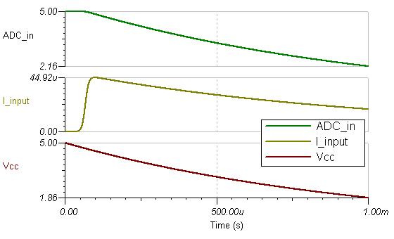
May I ask you to indicate recommended max Cin value for TLV2556 when the device faces power sequencing? Does TLV2556 tolerate Cin = 10nF on inputs during power down when these caps are being discharged through the device?

In the same line, please clarify whether TLV2556 total peak current spec refers to permanent current. If not, please specify relevant time period.

Many thanks,
Milan

Two days later: No reply.
August 30:         No reply.


  • Hello Milan,

    During power down, power supply capacitors don't allow fast discharge of supply pins. This keeps dissipation currents very low while the ADC input tracks the supply pin during power down. Thus, there is no need to worry about high discharge currents through the device from a 10nF cap.

    For example, the simulation below shows the discharge of a 10nF cap at 5V through a high current schottky when the supply discharge time constant is about 1ms, which is very common. To approximate 30mA of max discharge current, the supply discharge time constant will need to approximate 1us, which is not very common.


    Was the TLV2556 damaged after a power cycle? If this is the case, could you share with us the schematic of the design and a scope screenshot of the supply pin during power up and power down?

    This will help us to have a better idea of what is causing the issue. For privacy, the schematic can be send to me via a conversation by clicking “start a conversation” at my profile.

    Thank you,
    Rafael

  • Hello Rafael,
    Thank you for your thorough feedback.

    None of my ADCs were damaged. The only reason why I raised this question is that I I would like to build an ADC input conditioning circuit that meets all reqs imposed on SAR devices while making sure there is no potential risk in terms of power-up/down sequence whatsoever. 

    The App Note provide basic facts above SAR conditioning circuit, however, there is no info on power sequencing. That's why I decided to contact support team.

    Re your analysis -  I am afraid you need to multiply the estimated current by the number of ADC inputs as max peak of 30mA is a total sum specified for the entire device, am I correct? Only 20mA is allowed for each input I think.  

    Thanks and regards,
    Milan


  • Hello Milan,

    I’m glad there are no issues with the ADC.

    Regarding the current, yes, you are correct. The device is rated to dissipate current spikes of up to 30mA. For example, if three inputs dissipate 11mA of instantaneous current, each input is below the limits, but it is possible for the device to get damaged because the total current is 33mA. Therefore, it is safer to make sure that each input is current limited to 3.7mA spikes when there is an over-voltage or under-voltage.

    Fortunately, the 10nF cap shouldn’t create spikes close to those limits. With a typical 1ms power down time constant, each input would only dissipate about 50uA as max current spike, which is much lower than the limits.

    Based on my simulations, as long as the supply decay time-constant is more than 20us, each input current should be below 3mA with a 10nF@5V(worst case). However, it would be rare to have a supply decay this fast. This is why I don't believe 10nF capacitors will affect the ADC.

    Regards,
    Rafael

  • Hello Rafael,
    Thanks for your clarification.
    I think I understand your approach. No more questions at the moment.

    Let's consider this SR closed.

    Thanks again,
    Milan