This thread has been locked.

If you have a related question, please click the "Ask a related question" button in the top right corner. The newly created question will be automatically linked to this question.

ADS54RF63EVM board functionality testing

Other Parts Discussed in Thread: ADS54RF63EVM, ADS54RF63, ADS4149

Hi,

 I connected ADS54RF63EVM to Virtex 6 FPGA board. I am capturing the adc_diff_data into an IDDR, which is clocked by dry_clk. But, my data is observed on ChipScope ( Xilinx tool to see internal signals ) and is found to change NOT with respect to the dry_clock! 

1. data coming to the flip flop is not synchronous with the clock

2. I used the dry_clk inside the fpga, and sent it out via the sma_out of the FPGA board. It does not look like a sinusoid! Infact, it's shape changes with the frequency! Sometimes, it's close to a sine, otherwise it's something else !

 I have been trying on this ADC board for a long time now, and I tried different ways to debug the issue, such as combining ADC-FPGA-DAC, using flip flops to sample, using IDDR to simple ( the simplest way ). No issue has helped me to obtain a faithful representation of the ADC working!

 At this point, I seriously doubt if the ADS54RF63EVM board with me is in working condition or not! Using this board is extremely crucial for my work, and I would very much appreciate any help in this regard.

Thanks a lot in advance,

Basil.

  • Hi, 

     I tried testing only the ADS54RF63EVM board, with the breakout board provided along with it (J2).  I provided a 100 MHz sinusoidal clock with 0.7Vp-p (single ended) and a 15 Mhz sinusoidal input with 1Vp-p (single ended). I was measuring the bits from the breakout board with the help of a DSO probe. ( By placing the tip of the probe at the pin location, eg. A4 for MSB ).

    I observe that the MSB varies with same frequency as the input signal, and has similar shape. I can't quite understand about other bits. Most of them are very low signals, including the MSB.

    Is this an expected observation ? Please help.

    Thanks in advance,
    Basil.

  • Hi,

    All EVMs are tested before they are put into stock.  If there is a serial number inked-in on the EVM then from that number i should be able to bring up the FFT plot from the EVM testing. 

    But to see if the EVM is still functional at this time, the easiest way would be to use one of the Capture Cards that we also have available, such as the TSW1400, TSW1405, or the older TSW1200.  The TSW1405 is a low cost capture card that would quickly demonstrate the functionality and AC performance of the EVM given the clocking and input signal that you are providing to the EVM. 

    But apart from that, check your inputs to the ADC, particularly the clock and analog input signal.  From a screenshot from a scope using a high bandwidth scope probe, check that the signal into the ADCs are of sufficient amplitude and of the proper DC level as per the ADS54RF63 datasheet.  (That is, that the signal is differential and biased to the desired VCM.)   If you get scope shots of your input signals, post them and i will take a look at them.  Also, check the DRY with a scope.  it is not a sine wave, but an LVDS square wave of the same frequency as the sampling clock into the ADC.

    The LVDS data bits and clock *are* synchronous as they leave the ADC, plus or minus some possible skews as there are skew limits listed in the datasheet.   Using a scope on the signals from the ADC you should see the data transitions line up with DRY transitions to within some tolerance.  But using chipscope in the FPGA, you may be seeing the DRY delayed by some global buffer delay that the data bits don't have to have.  In fact, in the TSW1200 code when I set the delay settings for the IDELAY for the data and IDELAY for the clock, i only had to use 1 tap of delay on the clock to meet setup and hold into the IDDR cells.  The global clock buffer gave me the rest of the delay I needed.  Conversely, when i was setting IDELAY tap settings for a device with the clock *centered* on the data already such as ADS4149, then i had to use 10 tap settings on each data like to match the clock delay through the global clock buffer to keep the clock centered on the data when it got to the IDDR cells.  So clock buffer delays in the FPGA can be significant.

    Regards,

    Richard P. 

  • Hi,

    Yes, with a slow sine wave input relative to the clock, the msb looks like a square wave as the msb flips each time the differential analog input passes through its zero crossing.   The next msb does a low-high-low-high or high-low-high-low areound each of these same crossings.  then the next msb to this does a low-high-low-high-low-high around the transitions.  Each successive bit adds another pair of transitions, until you get to the middle and low order bits and then it gets too hard to pick out the pattern.   The slower the sine wave, the better able to see the patterns on more of the bits.  With a 15M input at 100Msps, then maybe only the msb would be recognizable.

    The AC coupling on the EVM will not let you pass through a very low frequency, but one way to get a 10KHz sine wave input to the ADC is to let aliasing do the work and alias the analog input down to a very low frequency.  So if sample clock is 100MHz, then an input of 100.010MHz to the analog input will come out like a 10KHz input.

    These are LVDS signals, so if you look at the signals with a high impedance *differential* probe then the typical signal swing would be about 700 mV peak to peak.  But if you are using a high impedance single ended probe on one side of the signal at a time, then the expected swing would be about 350mV.  if that is what you mean by very low signal, then yes this would be expected.

    Regards,

    Richard P.

  • Hi Richard,

    Thanks for the very very detailed reply. Yes, I do have a serial number inked on the EVM. The number is "126".

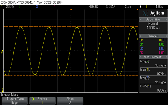
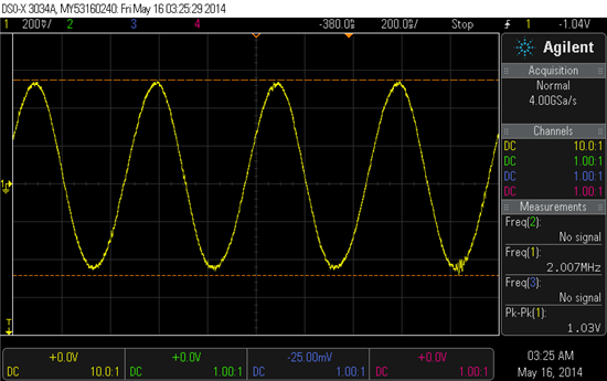
    The ADC input frequency I am probing at the clock pin of ADC EVM (J17) is 96 MHz, 0.93 Vp-p. The ADC input signal that I am giving at J11 has a frequency of 1.2 Mhz and 1 Vp-p. I will take a screenshot and attach it below respectively.

    Yes, I checked the DRY signal. For lower frequencies I got it as more of a square wave, while for higher frequencies I got it more as a sine wave. ( I assume it is because of the bandwidth of the scope. Please let me know if there could be some other reason).

    Changing the IDELAY tap setting - Will I be able to see the same in chipscope? Because, at the moment I am not able to see the effect!


    Yes, I am getting a pattern similar to what you mentioned in your second post. My MSB varies with same frequency as input. Next bit varies as a low-high-low-high signal, and so on.

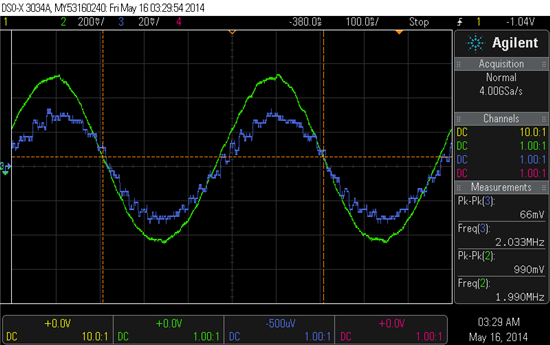
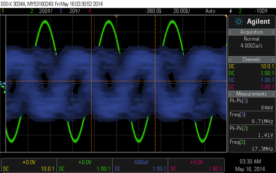
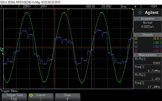
    PS : I am also attaching the screenshot of the input and output of my ADS54RF63-FPGA-DAC34SH84 system! I find from chipscope that my ADC digital output is noisy! You can also see it from the attached final analog output! I would like to know why these noise could appear? As I increase the frequency of the input signal, the noise at the output increases!

    Output (BLUE) when input (GREEN) is 2 mhz is shown in first figure. 


    Output (Blue) when input is 17.3 Mhz (green) is shown in following two figures!


    PPS : Thank you for your patience for helping me up to this stage. It has been very much positive!

    Regards,

    Basil.

  • After connecting the ADC to FPGA, I looked how the bits are varying using the chipscope. I get the following pattern.
    MSB varies at same frequency as input. Next bit is an inverted waveform of MSB! And, even LSB is not varying!

    Could this be a potential source for the noisy data that I am getting? Please find attached a screenshot of the same.

    Thanks a lot,

    Basil.

  • Hi Richard,

     It would be helpful if you could please look into the ADC MSB and next bit issue that I was mentioning. Also, the LSB is staying fixed when I view inside the Chipscope.

    Thanks,

    Basil.