Because of the Thanksgiving holiday in the U.S., TI E2E™ design support forum responses may be delayed from November 25 through December 2. Thank you for your patience.

This thread has been locked.

If you have a related question, please click the "Ask a related question" button in the top right corner. The newly created question will be automatically linked to this question.

ADS7954 / maximum source impedance with buffer between the MXO and AINP pins

Guru 20090 points
Other Parts Discussed in Thread: ADS7954

Hello,

In the datasheet P.40 of ADS7954, there the discriptuon about restrinction on source impedance.
Could you please let me know maximum source impedance with buffer between the MXO and AINP pins ?

Our customer added a common ADC driver buffer between the MXO and AINP pins with 1Mohms source impedance.
Then they faced bad linearity and THD.

Best Regards,
Ryuji Asaka


  • Hello Ryuji,

    The ADS795x is a typical SAR ADC.  As shown in the figure on page 23, SAR ADCs work in two phases:  A sampling (acquisition) phase and a conversion phase.

    During the acquisition phase, the ADC’s internal sampling capacitor is connected to the selected analog input pin. At the end of the acquisition phase the sampling switches are disconnected, storing a charge proportional to the input voltage. The device then enters the conversion phase, where an internal DAC and a comparator are used to determine the digital word corresponding to the input voltage.

    The acquisition time is dependent on the sampling frequency.  At fsample=1MHz, the minimum acquisition time is 325ns.   The driving circuitry must be able to charge the sampling capacitor array and settle to less than 1 LSB by the end of the acquisition time to maintain optimal performance.  The relation of the capacitor charging is exponential and related to the time constant formed by the series source resistance and the sampling capacitor.   Please find a slide from a presentation discussing this topic attached.

     4380.forum_sampling_cap.pptx

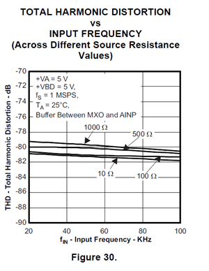
    As you have mentioned, the datasheet recommends limiting the source impedance to less than 1kOhm between MXO and AINP.  Figure 30 shows the THD performance  vs input frequency  across different source resistance values up to 1kOhm.

    The typical mux impedance between Chx and MXO is in the order of 200 ohms when CHx is on as shown on figure 59.

    Best Regards,

    Luis