This thread has been locked.

If you have a related question, please click the "Ask a related question" button in the top right corner. The newly created question will be automatically linked to this question.

TLC5540 -- DC level at ADC input creating errors

Other Parts Discussed in Thread: TLC5540

Hi,


We are using the TLC5540 chip on our board interfaced to a Virtex6 FPGA (Schematic attached).

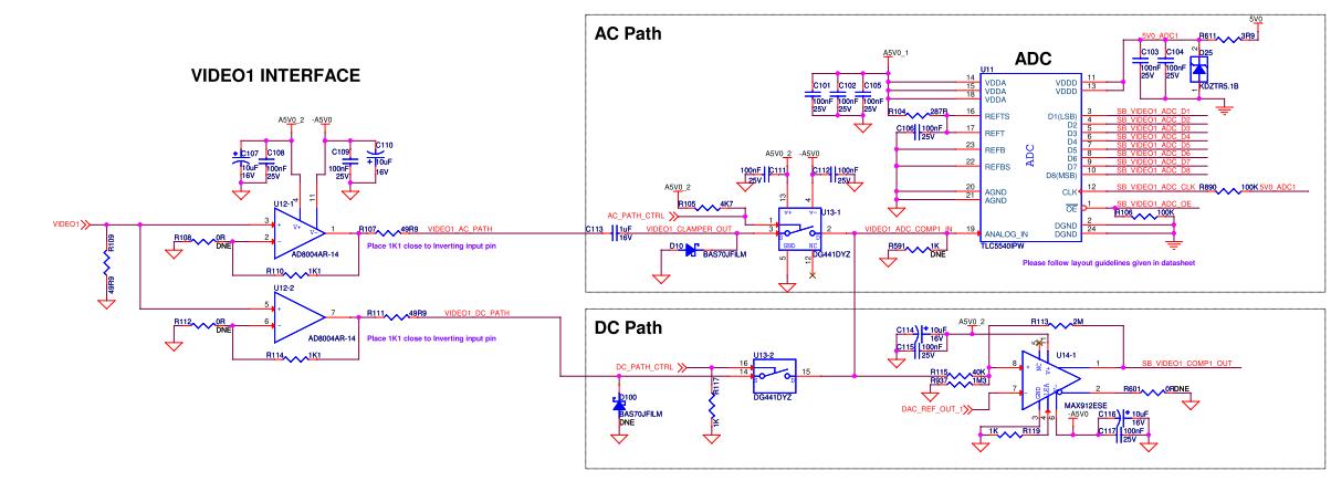
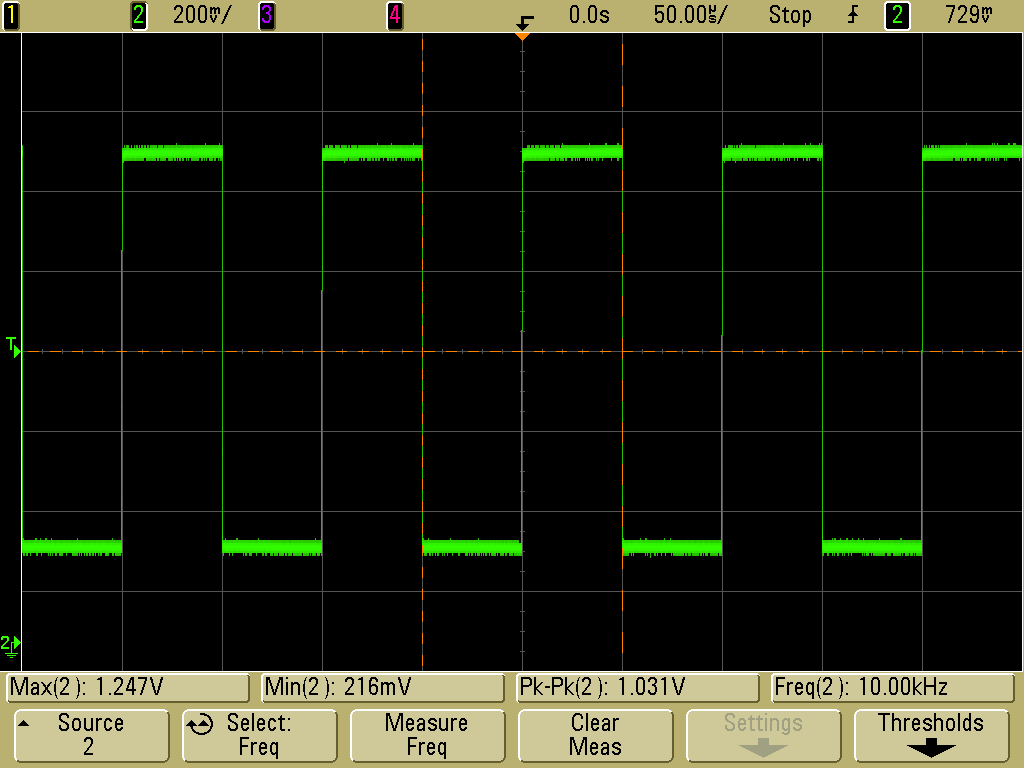
We are using it for sampling an input video signal fed from a Function Generator (with 50ohm output impedance) at 40MSPS. The circuit was working fine for over a week. Since yesterday, when we are feeding an input sinusoidal signal swinging between 0 to 3.2V at 10kHz through the AC path or DC path of the design, we are observing a DC shift of approximately 1.5V on the input signal at the ADC input. This, in turn, is causing errors in the data captured by the ADC.

To find the root cause of this problem, we tried isolating the analog input using the RF switch in between. We found that with no input signal applied to the ADC, a 1.5V DC voltage was still coming at the ADC input.

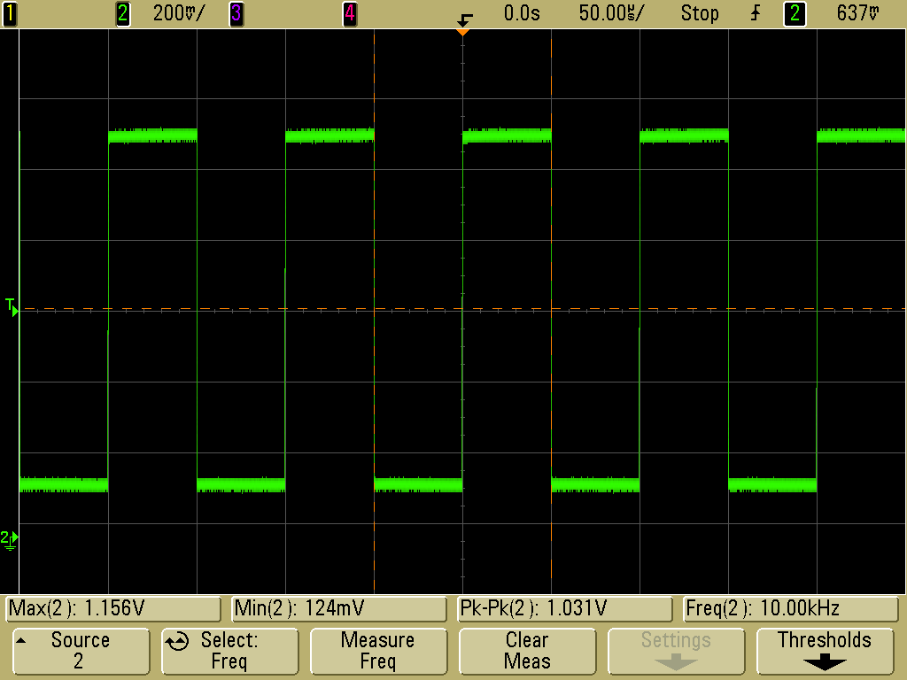
Since we had a comparator (MAX912) also in the path, we suspected the comparator to introduce this DC level. So we isolated the comparator input from the circuit by removing the series resistor R115.Still, a 1.5V dc was coming at the ADC input without any analog signal applied.

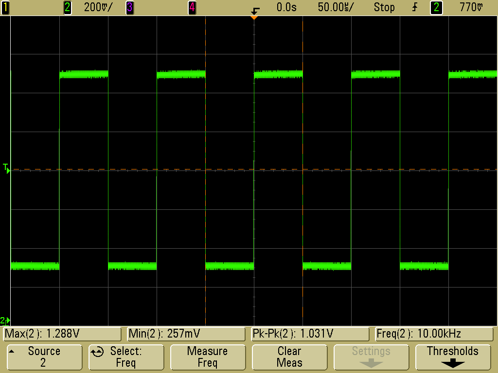
We had a provision to enable/disable the sampling clock to the ADC. When we disabled the 40MHz sampling clock to the ADC, we found that the DC level came down to zero. When the clock was enabled again, 1.5V dc started coming again at the ADC input.

Why is this DC level shift happening at the ADC input? What can I do to overcome this dc level shift from affecting the ADC data capture as well as other circuits?

Regards,

Avinash

  • Hi Avinash

    Are the +5V and -5V power supplies for the amplifier U12 at the correct levels?

    What is the voltage on each side of R111 when using the DC path?

    What is the voltage at pin 5 of U12?

    This information will tell us if the amplifier and analog switch are working properly, and how much current is flowing from the ADC input through R111.

    Best regards,

    Jim B

  • Hi Jim,

    Yes. The +5V and -5V power supplies to U12 are proper.

    At pin 5 of U12, the input swings between 10mV and 3.17V.

    At left side of R111, the signal swings between 40mV and 3.2V.

    At right side of R111, the signal swings between 40mV and 3.2V.

    The input signal applied from the function generator is swinging between 0 and 3.2V and a frequency of 10kHz.

    Regards,
    Avinash
  • Hi Avinash,

    It's not entirely clear if you're having issues with the AC path or the DC path (or both)...

    You mentioned that the circuit was working fine but now it's not working. Can you clarify what this means? What changed? Just the source? Can you change back to the previous configuration to verify it still works?

    I'm assuming the 1.5V offset is measured at the FPGA - after data is captured? Is it possible that the MSB has been dropped or is being interpreted correctly? This could result in an apparent 1.6V shift.

    If only the DC path is the issue, can you verify the voltage at pin 7? Has the DAC reference voltage (DAC_REF_OUT_1) been set correctly?

    Example captured data could be helpful as well.

    Regards,
    Matt Guibord
  • Hi Matt,

    My apologies for the ambiguities in the problem statements above. Let me clarify it further.

    We are facing the issue with AC path. No changes were done on the circuit or the board so far. Even the signal source as well as the input signal applied to the device is same as earlier. We tried to change back to the previous configuration too. But the 1.57V offset is always there at the ADC input pin.

    The offset voltage is evident when we probe the ADC input pin using DSO also. Please see snapshots below. These were taken with an input signal of 1Vpp applied to the circuit. (We have limited ourselves to work with 1Vpp signal now such that the input voltage doesn't go higher than the ADC's input range with the DC offset)

    1. Video input to AD8004

    2. Input to analog switch in AC path

    3. Output of analog switch in AC path

    4. Input to analog switch in DC path

    5. Output of analog switch in DC path

    We have tried varying the DAC ref voltage from 0 to 2V. But the response has been the same always. Also, to isolate the issue further, we have tried isolating the 40k resistor (R115) and also pins 2 & 15 of the analog switch DG441 from the ADC input. The ADC input still shows the 1.57V offset when probed in the oscilloscope.

    When the clock is not driven from FPGA, the offset drops down to zero. But when the clock signal is applied, even when no other circuit is connected to it, the ADC shows 1.57V offset always.

    Regards,

    Avinash

  • Hi Avinash,

    I guess I'm confused here - note that I am not an expert on analog video signals... For the AC path, you're only trying to measure the AC response. Your reference range is roughly 0V to 3.2V. Therefore you need to bias the ADC at 1.6V to maximize the AC swing you can measure. This is exactly what your circuit seems to be doing... Why is this an issue?

    If you can provide a description of exactly what you expect the circuit to do, I may be able to help. It's not clear to me what the AC and DC paths are used for. Are the AC and DC switches closed at the same time? Do you alternate which is open and which is closed?

    I think you need to simulate your input circuit to see the response that it is providing. I have a feeling that the input circuit is the issue. The ADC does not set the DC bias at the input, take a look at figure 13 in the datasheet to see that it is high impedance. The ADC will have no effect on the DC voltage seen at the ADC input. A spice program such as TI-TINA will allow you to simulate your circuit to see what the expected voltage is at the the ADC input.

    Regards,
    Matt Guibord