This thread has been locked.

If you have a related question, please click the "Ask a related question" button in the top right corner. The newly created question will be automatically linked to this question.

TLV2556 Crosstalk

Other Parts Discussed in Thread: TLV2556, OPA322, OPA4322

Hello,

I am using theTLV2556 in a new product. I'm seeing some crosstalk across channels and realized that I'm violating the chip’s analog voltage input range by going below -0.3 and above Vcc + 0.3. I have design choices so I have a couple questions:


  1. Exceeding VREF. The datasheet recommends that the analog voltage not exceed VREF. If I exceed VREF but do not exceed VCC I know that the converter will output maximum count but is there any risk of crosstalk?
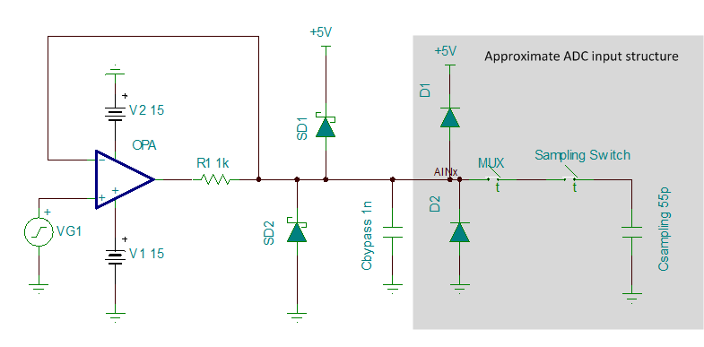
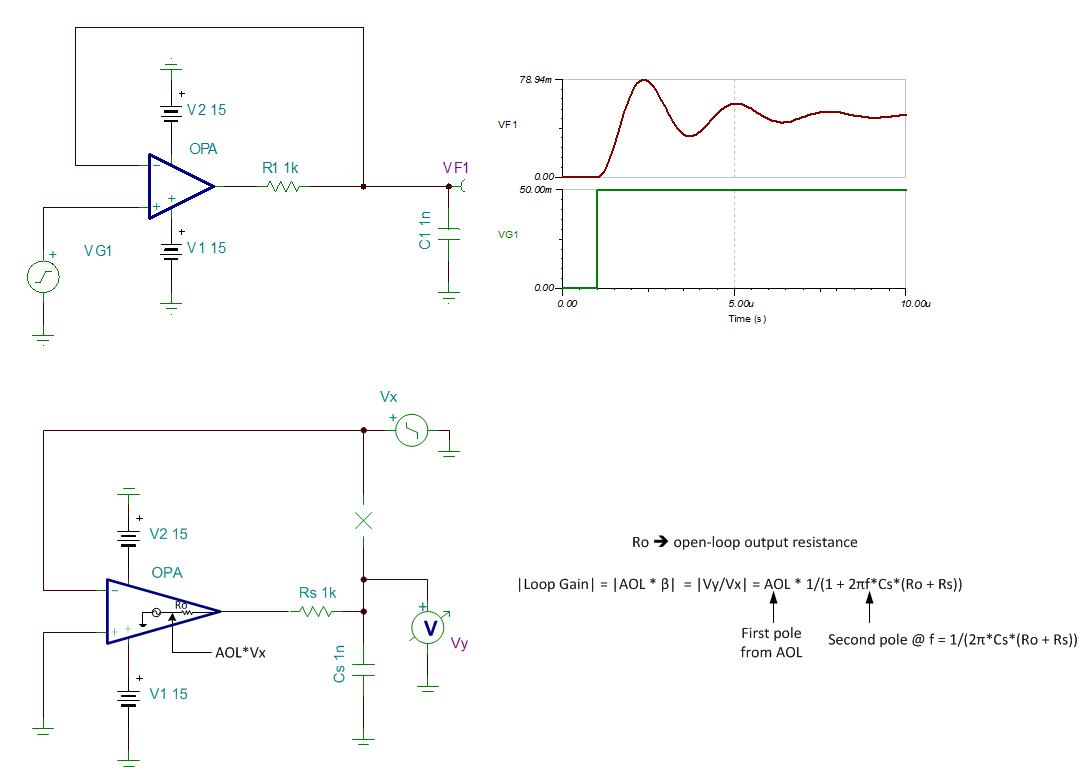
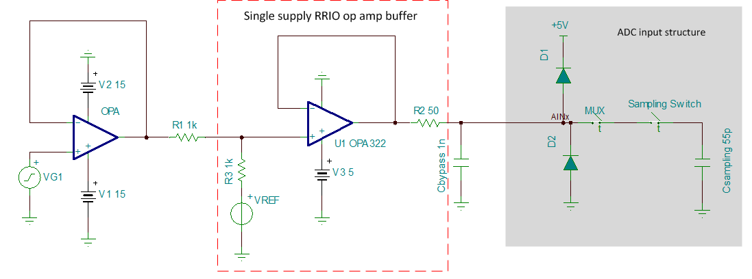
  2. I’m using opamps powered by +/-15V that present voltage to the TLV2556. We are using series resistance and clamp diodes to VCC and ground. I can keep the analog input voltage to the converter within limits by using better performing diodes  and increasing the series resistance to 1k ohm. Does this create a potential problem? I noticed that the Analog input MUX impedance can be as high as 600 ohms but I’m not sure what this is.

Thank you for your help.


Russell

  • Hi Russell,

    1) Crosstalk vs. input voltage is not something that's been characterized on this device, but generally speaking crosstalk is an AC coupling phenomenon and I would think it is more dependent on input frequency rather than amplitude.

    2) Input source resistance presented to the ADC has a direct impact on its linearity (or accuracy). Basically, the MUX is just an array of analog switches. The input leakage current as well as the on-resistance of an analog switch (600ohm max in this case) are non-linear functions of the input voltage. The input leakage current drops voltage across the series input resistance and introduces a non-linear voltage error between the output and input of the switch. The non-linearity in the switch output subsequently carries over to the ADC output and thus the ADC output becomes a distorted representation of the input signal. Adding series input resistance only increases the distortion in the ADC output and makes the ADC less accurate.

    Best Regards,
    Harsha

  • Hi Russell - Thanks for submitting my question.

    Hello Harsha -

    I'm trying to assist colleagues at another location. Basically we have a couple scaling amplifiers, powered by +/-15V, that feed into analog channels via a current limiting resistor and clamp diodes to ground and 5V. They tested by applying a slow ramp voltage to one scaling amplifier and see the A to D voltage rise and then flatten when the scaled voltage = VREF+. This is expected. They continue to drive the voltage up and at some point, the voltage jumps up on another channel (where there has been no change to its input). This is what I referred to as crosstalk and may not be the correct term.

    I looked and noticed that they were using clamp diodes that would quickly violate the chip maximum limit of VCC + 0.3 or 5.3V. I found a better performing diode and increased the current limit resistor from 100 to 1k to further reduce voltage drop and hold the analog channel voltage to limits. I now know that this isn't a good idea.

    Two questions for you:

    1. Is this overdriving of the analog input causing the rise in voltage on another channel? If not, what would cause it?

    2. Can you recommend a better pair of components to use for the clamp?

    Best regards

    - Bill

  • Hi Bill,

    The behavior seems unusual but I will need more detail to clearly understand what is being observed and what kind of debug measures have been taken. A few questions:

    - Could you post a schematic that clearly shows the ADC input signal path and describe the signal at the op amp inputs (DC offset, amplitude, bandwidth)?

    - As for the coupling behavior, is the jump observed on all channels or only some of the channels and at what value on the ramp (past VREF) does the fault occur?

    - Are the affected channels floating (or driven though high source impedance) when the fault condition is observed and to what value does the voltage jump?

    - Can this behavior be replicated on a different channel under the similar conditions?

    Best Regards,
    Harsha
  • Hello Harsha -

    Thank you for the response. I was not able to duplicate my colleague's results, so I am still gathering info. I do have a question. What type of behavior should I expect from the TLV2556 if an analog input violates the VCC +0.3V limit?

    Cheers!


    - Bill


  • Hello again Harsha -

    A follow up question to your original response.

    Regarding leakage current and the resulting voltage drop. The TLV2556 datasheet identifies Selected channel leakage current as sinking or sourcing 1uA max. Is this the leakage current that you are referring to?

    Saludos!

    - Bill
  • Hi Bill,

    Taking the input over 300mV above VCC will forward-bias the internal ESD clamp to VCC, and the input pin will experience a strong pull-down load (as intended). The VCC pin will sink a large current from the input source possibly causing it to current limit. If the VCC current sink is large enough to exceed the max power handling capability of the clamp circuit then the ESD clamp circuit will heat up and burn. Bottom line - if you're monitoring the part's supply current you should see it surge.

    Best Regards,
    Harsha

  • Hi Bill,

    I believe that is the very same parameter, and at 1uA max it would take a 1.2kohm resistor to create a 1LSB error (5V/2^12 = 1.22mV), which as I recall, is about the value you were considering to limit the current through the external diodes in an over-voltage condition. Anyway, input distortion aside, it is still important to keep the source impedance low to ensure that the input voltage settles completely (to a 12-bit level) across the sampling capacitor before the start of conversion.

    I was talking to my colleagues over in op amp applications about how to limit op amp output current without substantially increasing the ADC input source resistance and a good suggestion I received is to place the current limiting resistor in the feedback loop of the op amp. This would not only provide current limiting but also attenuate the source impedance into the ADC by the loop gain of the op amp. The complete circuit is shown below:

    Sounds like you might already have something similar but SD1 and SD2 are high current schottky diodes (similar to the BAT54S) that would conduct most of the nearly 10mA (or 15mA for SD2) out of the op amp output if the voltage rails. Note that this would have to be done on every MUX input.

    Best Regards,

    Harsha

  • Hello Harsha -

    Thank you for the example circuit and explanation. I agree that the opamp in this configuration would compensate for any error due to the leakage current and a good idea. I'm presently using BAT54S but a bit concerned about forward voltage part to part and over the temperature ranger. One of my colleagues suggested that we use the 4.096V A to D reference as the clamp source. I'm not sure I like this but the reference that we are using can maintain regulation while sinking or sourcing up to 10 mA. What do you think of that?

    One more follow up question about driving the analog signal above the 5.3V limit. You described how the over stimulated input would respond but should everything else behave normally? In other words if one channel is in a fault condition and the TLV2556 is instructed to read another channel that is in normal range, will the TLV2556 report correct voltage? Will the timing be normal?

    Cheers!

    - Bill
  • Hi Bill,

    I don't think clamping the inputs to the reference source is a very good idea because the current limit would be too low to clamp all 11 input channels.

    On the other hand, the +5V supply would make a much better clamp source, provided that it can sink current. Most LDOs cannot sink current and so a TVS diode in parallel with the LDO output is typically necessary to provide a lower impedance clamp.

    Going back to my previous message, I had further discussions with my colleagues about the idea of placing the current limiting resistor in the op amp's feedback loop, and while we do get the benefit of lower effective source impedance (or equivalently, error correction at the MUX input as you put it), the biggest trade-off is op amp stability. The resistor does not provide any isolation of the op amp output from the cap load. As a result the op amp loop gain will now contain 2 poles (one from AOL and the other due to Cs) within the unity gain bandwidth which degrades phase margin and causes the op amp output to oscillate.

    Of course, the op amp can be compensated but improved stability comes at the cost of bandwidth, and this pretty much means that the op amp output will not fully settle during the minimum 600ns acquisition window, which once again causes accuracy issues. So basically the resistor cannot be placed in the op amp's feedback path, and we're now back to the original problem of simultaneously achieving current limiting as well as settling accuracy.

    The only way to meet both design requirements would be to introduce a buffer that uses a single-supply op amp between the high voltage op amp and the ADC. The complete circuit is shown below:


    The OPA322 (which is linear to within 100mV of the rails) has robust input protection that can easily withstand +/-10mA continuously. This would eliminate the need for any external clamping circuits. Also, since the source resistance seen by the 1nF is very low, the ADC inputs would now settle to a 12-bit level well within the minimum acquisition time (600ns). A quad version of the OPA322 (the OPA4322) is also available. The only drawback would be that because of the 100mV swing to rail limitation, the output of the OPA322 will not be able to provide 0V.

    Transient simulation of the settling behavior is attached.

    Regards,

    Harsha

    TLV2556_OPA322_settling.TSC

  • Hello Harsha -

    Thank you for digging into this and providing such a thorough analysis. My lesson learned is to drive the A to D with an amplifier connected to the same voltage rails as the A to D. I have no more questions about protection schemes.

    Best regards


    - bill