This thread has been locked.

If you have a related question, please click the "Ask a related question" button in the top right corner. The newly created question will be automatically linked to this question.

DAC3164 Input Requirements

Other Parts Discussed in Thread: DAC3164, DAC3283, DAC3171, DAC3174, DAC3154

Hi team,

We're interested in using the DAC3164 in our design and had a couple questions:

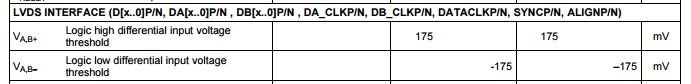
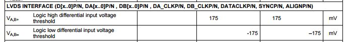
  1. Most FPGAs guarantee Vod (output differential) of 250 mV. Looking at the datasheet of the DAC3164, we see a minimum input differential swing of 350 mV. Could you please confirm this requirement?

  2. For the DACCLKP/N, it says "LVPECL clock input for DAC core with a self-bias of approximately CLKVDD18/2" which is approximately 0.9 V. However, for the Input Common Mode Range is says minimum of 1.0 V. Do the AC coupled DACCLKP/N inputs require external biasing?
  3. In the DAC3174EVM, ALIGNP/N is connected to a clock generator output. Why is this the case? In the datasheet it says "It is used to reset the clock dividers and for multiple DAC synchronization. If unused it can be left unconnected."

Thank you,

Akash Patel

  • Hi.

    1)  I believe most FPGAs would guarantee an LVDS output swing of 250mV peak, rather than peak to peak differential.  An LVDS output is nominally 3.5mA through a 100 ohm load, for a swing of 350mV.  but that is +/- 350mV, as a logic '1' would have the 3.5mA flowing in one direction for a voltage across the 100 ohm resistor of 350mV, while the logic '0' would have the 3.5mA flow the other direction, for a voltage of -350mV across the resistor.  nominal peak to peak differential LVDS swing would be 700mV, or just 350mV swing if you just look at one side of the differential pair.  The DAc3283 datasheet has more documentation than the DAC3164 datasheet, and includes a figure to illustrate what the datasheet author is trying to say in 47 of page34 of that datasheet.    In that figure they assume a nominal swing of 400mV instead of the 350mV I am more used to seeing, though.   But they illustrate what they mean by the VAB.   If +/-350mV is a common LVDS spec, +/-250mV would be a reasonable min.   I've not seen any LVDS drivers that would only guarantee 250mV peak to peak - that is smaller than many receiver's differential sensitivity. 

    So the DAC3164 is specifying a requirement of at least 350mV peak to peak differential, smaller than the usual 500mV peak to peak VOD min of FPGAs.  We have not trouble for example driving the DAC3164 with the usual LVDS driver of the Altera FPGA that is on our TSW1400 Pattern Generator Board, or the Lattice that is on our TSW1406 Pattern Generator Board.

    2) The DACCLK does self-bias to approximately 0.9V.  But the DACCLK is not an LVDS input, like the DATACLK and so the second note that you mentioned of having a minimum 1.0V does not apply to DACCLK, just to the LVDS inputs.  The DACCLK expects an LVPECL swing that is then AC coupled and terminated at the DAC.  After the AC coupling, the DAC3164 will bias the LVPECL down to where it wants to see it.   Again, I have to point to the DAC3283 datasheet for clarification on the DACCLK.  The specs for the DACCLK got left out of the DAC3164 data sheet and are being added in now. (I am proofreading the 3161 datasheet now, and 3164 datasheet would be next.)  Figures 44 and 45 of the DAC3283 datasheet illustrate the DACCLK input structure and recommended termination.  And the DACCLK electrical specs are on page 9 of that datasheet.  The DAC3164 and DAC3283 are the same CMOS process and use the same input circuit and so the information that did make it into the DAC3283 datasheet is being added to the DAC3164 datasheet.

    3) I do not know about the EVM, that EVM was created by someone before me.  But I do see that the characterization board that the characterization engineer made for lab characterization also had the ALIGN pins driven by the clock chip, *if* the output of the clock chip was even enabled.  I suspect that the EVM copied from the characterization board, and that the characterization engineer had a reason for it.  I can ask the characterization engineer what her reason for that was.

    Regards,

    Richard P.

  • Hi Richard,

    Thank you for your response. Referring to the datasheet snippet from above for the LVDS Interface, D[x..0]P/N, DA[x..0]P/N , DB[x..0]P/N , DA_CLKP/N, DB_CLKP/N, DATACLKP/N, SYNCP/N, ALIGNP/N are all listed in the LVDS section. Which inputs should be treated as LVPECL?

    Also, please follow up regarding the EVM after talking to the characterization engineer.

    Thank you,

    Akash Patel

  • Hi,

    The DACCLKP/N and the ALIGNP/N are not LVDS inputs but rather are LVPECL inputs.  Please note on Figures 1 and 2 that the LVDS inputs and LVPECL inputs are identified.  Also the pin assignment tables (page 5 and page 7) reiterate this. 

    But since the original datasheet omitted the electrical spec section for the LVPECL inputs entirely, I can see where the uncertainty arises about which pins are LVDS or LVPECL.  This is being fixed in the datasheets, as I am editing the DAC3171 at the moment and the other datasheets in the family are in edit phase as well.

    Note that the DACCLKP/N is *not* listed in the list of LVDS signals D[x..0]P/N, DA[x..0]P/N , DB[x..0]P/N , DA_CLKP/N, DB_CLKP/N, DATACLKP/N, SYNCP/N, ALIGNP/N.   But adding to the confusion - the ALIGNP/N is listed in with the LVDS signals and this is an error as well since ALIGN is not LVDS.  And the signals:  DA[x..0]P/N , DB[x..0]P/N , DA_CLKP/N, DB_CLKP/N are not signals in the DAC3164 or DAC3154 at all.  These don't even exist in this data sheet.  These *are* signals in the DAC3174 datasheet, as it is the DAC3174 that allows the data bus to be split into two 7bit busses for channel A and channel B, and so the D[x..0]P/N gets split into DA[x..0]P/N , DB[x..0]P/N, but not for DAC3164.   This all came about by having an original datasheet for the DAC3174 that had all the options available, and then spinning the 1-channel datasheet out of the original and spinning the 12 and 10bit datasheets out of the original and stuff like this didn't get fully edited out.  This is all being mopped up now.  And the electrical specs section is being added under a heading that will say:

    LVPECL DIGITAL INPUTS (DACCLKP/N, ALIGNP/N).

    I also spoke with the characterization engineer as to why the ALIGN pin is connected to the clock chip.  Actually, the characterization board allows for 2 or 3 different sources to drive the ALIGN pin for characterization, one of which is the clock device and another is the Samtec connector that the sample data and clocks all pass through.  The primary usage was to have a parallel vector signal generator drive pattern sets through the connector to the DAC which also include the ALIGN signal.  

    But note the two clock domains involved; the sample clock and the data clock.  On the input side of the DAC FIFO there is the data clock, and the data bus needs to meet setup/hold times around the data clock, and the SYNC input also falls on this side of the FIFO.  The SYNC inputs if used also need to meet setup/hold timing around the data clock. 

    The other clock domain is the sample clock DACCLK.  The output of the FIFO is driven by DACCLK, and the ALIGN signal falls on *this* side of the FIFO.  So the ALIGN pins (if used) need to meet setup/hold time around the sample clock.  The ALIGN signal is used to reset the output pointers of the FIFO, particularly in the case where you wish to synchronize multiple DAC devices. The ALIGN signal could be periodic by a multiple of 8 since the FIFO is 8 words deep, so the ALIGN signal could reset the output pointers every 8 or 16  or 24 (etc) clock cycles.  And since it needs to meet timing relative to DACCLK, the clock chip could be used to source DACCLK and the ALIGN signals.   The EVM stripped out the circuitry that let the parallel vector pattern generator drive test vectors to the DAC, but left the clock chip as a possible source for ALIGN.  We rarely use the DAC EVM in a setting where we synchronize multiple EVMs, so I have not used the ALIGN signal.

    Regards,

    Richard P.

  • Thankyou Richard.
    This clears all my questions.

    Ashok