This thread has been locked.

If you have a related question, please click the "Ask a related question" button in the top right corner. The newly created question will be automatically linked to this question.

ADS5281 EVM output signals after do reset command via SPI software

Other Parts Discussed in Thread: ADS5281

I'm working on a ADS5281 EVM interfacing with Xilinx Virtex5.

The main sampling rate was 50 MHz given from FPGA.

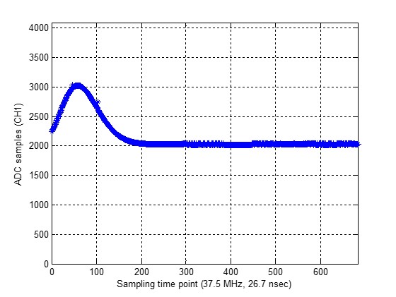
I'm wondering why I could see the output ADC signal (as following figure) with reset command via SPI software and no input analog signal.

Is it right? What kind of ADC output signal can be extected without any input analog signal?

I think this background signal affects the ADC output signal when I feed an anlog gaussian signal to ADS EVM.

In FPGA, I got two correct frame and bit clocks, but the deserialized data of each channel has only two or three distinct adc values (like 0, 2046, 4095).

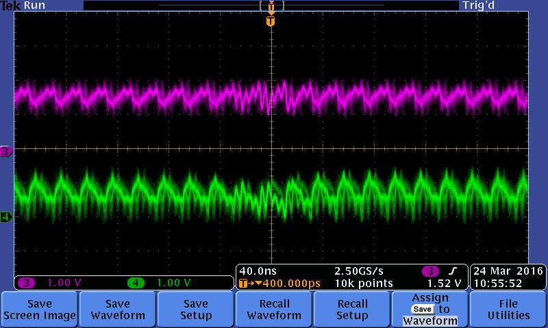
If I use 'Deskew' or 'Sync' test pattern, I could see clear Deskew or Sync ADC outputs on osciloscope.

But if I gave a command, "reset" by SPI software to feed an analog input into ADS EVM, I can't get a correct signal on oscilloscope and fpga chipscope.

Please give me some comments on how to start ADS EVM correctly with an analog signal or if there is some steps I missed.

This is the procedure how I start the ADS EVM:

1. power on ADS 5281 EVM
2. connect the usb of EVM to my PC (windows7)
3. perform "reset" command by SPI software.
4. check the output adc signal on osciloscope
5. give a command of "Sync" test pattern on SPI software
6. check the output adc signal on osciloscope
7. perform "reset" command by SPI software.
8. feed an gaussian analog signal to ADS EVM
9. check the output adc signal on osciloscope

Thanks,

Soo Mee.

  • Hi,

    The expected ADC output with no analog input (or analog input unconnected or floating) is that a few of the least significant bits of the output samples would toggle randomly.  Depending on the resolution of the ADC, maybe two least significant bits or maybe three bits would toggle randomly.  This would be called idle-channel noise.  But you would not be able to see that this is just idle channel noise until you deserialized the data from the LVDS lane and then could look at all of the 12 bits of the sample data.    Looking at the LVDS serial data on the scope will not tell much.  Then later if you apply a sine wave or some other signal to the analog input you would not be able to tell much from the serial data on a scope until you deserialized it and could look at the individual bits.   If you did tell the ADC to output the SYNC pattern then that pattern should look good on the scope - it would look just like the frame clock output.   Or if you used the custom pattern to make the output sample be something like 0000 0000 0001 then this should also be recognizable on the scope.    Using custom pattern to output 0000 0011 1111 should also look like the SYNC pattern and should also look like the frame clock.   Setting the custom pattern to 0101 0101 0101 should make the pattern on the scope show maximum toggle rate.

    Make sure the SPI GUI setting for the ADC is for differential clock after reset, as the EVM will convert the clock to differential.

    But once you start applying a real analog signal I don't think the scope will be too helpful.  you will need to deserialize the data.

    Regards,

    Richard P.

  • Thanks a lot, Richard.

    I could see the correct signals on scope and on deserializer with test mode (like SYNC or Deskew),

    but turning off test mode by SPI or connecting analog input to EVM make me so confuse.

    Because they are shown very unexpected signal on scope and on deserializer.

    I have one more question about reset command by SPI GUI.

    You said after reset, EVM will convert the clock to differential.

    Does that mean I don't need to give a differential clock to EVM?

    Since EVM has a pin of p-side of inclk, I connected p-side of 50MHz differential clock to EVM.

    The 50MHz clock was generated from FPGA DCM and then it was converted into differential clock signal.

    I'm wondering whether the input clock and analog signal into EVM must be differential signal or not.

    Thanks again,

    Soo Mee.

  • Hi,

    check the datasheet for the device, and check the user guide for the EVM that you are using.  The datasheet states that the default for the sample clock is single ended:

    "The ADS528x is configured by default to operate with a single-ended input clock—CLKP is driven by a CMOS clock and CLKN is tied to '0'. However, by programming DIFF_CLK to '1', the device can be made to work with a differential input clock on CLKP and CLKN"

    But the schematics of the User Guide and the text of the user guide describe how the clock into the EVM is single ended coax and is then transformer coupled to convert to differential to the ADC:

    "In the default case, a single-ended clock is converted to a differential clock using a Mini-Circuits TC1-1T transformer. When using this option, the ADC should be configured in differential clock mode by writing 0x8001 to ADC register address 0x42. By default, after a software reset this option is asserted to coincide with the EVM default."

    So after a hardware reset the ADC must be set to accept a differential clock.  I think the software reset button of the SPI GUI will automatically do this for you when you click the reset, but you would want to read the log of address/data operations shown in the SPI GUI after a reset to make sure that this is true.   I tend to make sure and click the button for clock diff/single-ended a couple of times to make sure I leave it in the diff state. 

    Regards,

    Richard P.

    The ADS528x is configured by default to operate with a single-ended input clock—CLKP is driven by a CMOS

    clock and CLKN is tied to '0'. However, by programming DIFF_CLK to '1', the device can be made to work with a

    differential input clock on CLKP and CLKN

  • Thanks a lot, Richard.

    As you recommend, I read carefully datasheet of ADS5281 and I captured deserialized adc samples of Gaussian analog input as following figure:

    x-axis is time sample point and y is 12 bits unsighed decimal values after deserialize.

    The gaussian analog input has a height of 400 mV and 0V offset.

    The result from the ADC gave a gaussian curve between -1 and 1 V (2 Vpp).

    Can I get the sample values betwee 0 to 2 V range?

    I found a data output format modes, BTC_MODE which has two straight offset binary and binary two-'s complement modes.

    Is BTC_MODE related to dynamic range of output data?

    Best,

    Soo Mee.

  • Hi,

    Offset binary and two's complement are just two different ways of representing the same digital sample value.  The only difference between them is that the most significant bit is inverted between the two.  if you have a sample value in offset binary and you invert the most significant bit then that sample code becomes 2's complement.  if you invert the msb again then the code becomes offset binary again.   Since the input analog voltage is differential, ranging between -1V and +1V differential, then at the minimum input voltage of -1V differential, the output code would start at 0000 0000 0000 and as the input voltage rose and crossed midscale, the output code would rise from 0000 0000 0000 and would cross midscale going from 0111 1111 1111 to 1000 0000 0000.   In 2's complement, the output is the same except the msb is inverted.

    if your input signal is smaller than full scale and you want to use the full scale range of the output codes, then you can use the SPI to set internal gain, as described in table 7 of the datasheet.

    Regards,

    Richard P.

  • Richard,

    I looked through table 7 in datasheet.
    But there is no explain of how to operate the gain.
    May I ask more explanation how to operate the gains?

    Does this gain amplify the input analog signal (gaussian, height:400mV) and then the full scale range can be changed?
    I'd like to express digital values (like unipolar binary) of my analog input within 0 to +2Vpp corresponding to Ox0000 and OxFFFF.
    Now the digital values are expressed between -1V and +1V corresponding to Ox0000 and OxFFFF.
    To express analog signal within 0V and +2V, how to set the gains or is there another way?

    Best,

    Soo Mee.
  • Hi,

    if you use register address 0x2A and 0x2B to set a gain value for a channel as in that table, then it would be like having an amplifier with that gain setting before the ADC.  For example, if you set a gain of 6dB, then instead of 2V p-p being the full scale for the channel, then 1V p-p would become full scale for that channel.   Using the gain setting would let you take a smaller signal input and gain it up to where it takes up more of the 12 bit sample values, but it will not also do any shifting of the signal - just gain.     So if you had an input signal that would swing from 0V differential to +400mV differential, then you could apply 6dB of gain and use more of the 12bit range, making it look like the signal would swing from 0V to +800mV.  But if you applied much more gain then you would begin to clip the signal on the top end but you would not be able to 're-center' the signal to use the whole -1V to +1V full scale range using gain alone.  You would have to externally condition your signal to make it swing from -1V to +1V differential in order to use the whole 12 bit range of the device. 

    Regards,

    Richard P.

  • Thanks, Richard.

    If I'd like to have 12 bit full scale digital outputs of an analog signal swing from 0V to 2V, how to do that?

    Now I got digital values of an analog signal from -1V to +1V.

    Do I have to change the condition of the input analog or can I do that by ADC register setting?

    Please teach me once more.

    Best,

    Soo Mee.