This thread has been locked.
If you have a related question, please click the "Ask a related question" button in the top right corner. The newly created question will be automatically linked to this question.
I use a CC2530 board connect with the ADS1299EEGFE-PDK daughter board.
I read chipID and got correct value.
Then I I wrote and read configs according to datasheet page 62(Setting the Device for Basic Data Capture )
In fact,I read some previous posts. According the post of Ivan Rock.(ADS1298: Run Test Signal and measure heart rate using two electrodes)
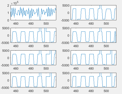
I read 27 bytes from buffer a lot of times,and form a [n x 8] matrix to store the signal.And I use the matlab test the internally test signal.
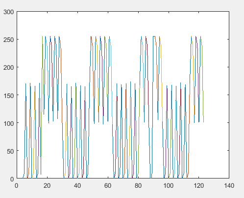
Here is my data and the image of a channel. The image looks like square-wave? AM I WRONG?
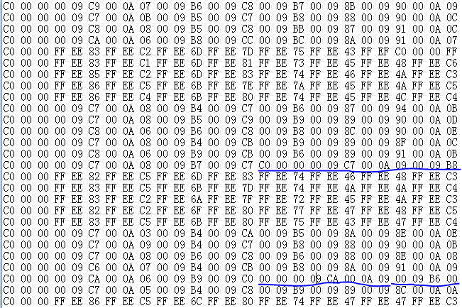
C0 00 00 00 09 C1 00 09 FF 00 09 AF 00 09 C2 00 09 B0 00 09 83 00 09 84 00 0A 03
C0 00 00 00 09 C1 00 0B 80 00 00 00 13 86 00 13 FE 00 13 58 00 13 84 00 13 52 00
C0 00 00 00 09 C1 00 09 FF 00 09 AA 00 09 C3 00 09 AF 00 09 83 00 09 88 00 0A 06
C0 00 00 00 09 BE 00 09 FE 00 09 AA 00 09 C0 00 09 AC 00 09 81 00 09 88 00 0A 00
C0 00 00 00 09 C0 00 09 FC 00 09 AE 00 09 C1 00 09 AD 00 09 7F 00 09 89 00 0A 03
C0 00 00 FF EE 7C FF EE BA FF EE 67 FF EE 79 FF EE 66 FF EE 3C FF EE 40 FF EE BB
C0 00 00 FF EE 7E FF EE BF FF EE 68 FF EE 7A FF EE 6A FF EE 3E FF EE 43 FF EE BD
C0 00 00 FF EE 77 FF EE BA FF EE 64 FF EE 79 FF EE 68 FF EE 3C FF EE 40 FF EE BB
C0 00 00 FF EE 7C FF EE B6 FF EE 63 FF EE 74 FF EE 67 FF EE 3B FF EE 40 FF EE BB
C0 00 00 FF EE 78 FF EE B9 FF EE 67 FF EE 77 FF EE 67 FF EE 3D FF EE 42 FF EE BB
C0 00 00 FF EE 79 FF EE BA FF EE 64 FF EE 77 FF EE 69 FF EE 3B FF EE 3C FF EE B9
C0 00 00 00 09 BE 00 09 FC 00 09 B1 00 09 BE 00 09 AE 00 09 81 00 09 83 00 0A 00
C0 00 00 00 09 BD 00 0A 01 00 09 AF 00 09 C1 00 09 AF 00 09 82 00 09 89 00 0A 03
C0 00 00 00 09 C0 00 0A 01 00 09 B1 00 09 C1 00 09 B1 00 09 85 00 09 87 00 0A 03
C0 00 00 00 09 C0 00 0A 01 00 09 AD 00 09 C0 00 09 AC 00 09 82 00 09 86 00 0A 08
C0 00 00 00 09 C0 00 09 FF 00 09 AD 00 09 C1 00 09 B1 00 09 83 00 09 8B 00 0A 01
C0 00 00 FF F3 04 FF F3 44 FF F2 F0 FF F2 FE FF F2 F4 FF F2 CA FF F2 CB FF F3 42
C0 00 00 FF EE 7F FF EE BD FF EE 66 FF EE C0 00 00 FF EE 7E FF EE BC FF EE 65 FF
It sounds very resonable!
But when I change the SPI clock ,it looks like invalid! And I'm not clearly know how to decrease the delay between the time DRDY asserts and you begin reading data.
Even I set the channel power-down,the zero-line has fluctuation.
Here is my code,could help me check my code and point out my fault!
#include <ioCC2530.h> #include <string.h> #include "hal_cc8051.h" #define LED1 P1_0 #define LED2 P1_1 #define SPI_DRDY P1_2 #define CLKSEL P1_3 #define SPI_START P0_6 #define PWDN P0_5 #define RESET P0_4 #define LED_OFF 1 #define LED_ON 0 #define TX_SIZE 20 #define TEST_DATA "test uart" char TxData[TX_SIZE]; void InitUart(void) { PERCFG = 0x00; // P0SEL = 0x0c; //P0_2,P0_3 P2DIR &= ~0xC0; //P0 UART0 U0CSR |= 0x80; //UART U0GCR |= 11; U0BAUD |= 216; //115200 UTX0IF = 0; LED2 = 1; } void UartSendString(char *Data, int len) { int i; for(i=0; i<len; i++) { U0DBUF = *Data++; while(UTX0IF == 0); UTX0IF = 0; } } void WriteData(uint8 command) { U1DBUF = command; while (!U1TX_BYTE); U1TX_BYTE = 0; } char ReadData(uint8 value) { U1DBUF = value; while (!U1TX_BYTE); //while (U1RX_BYTE); //U1RX_BYTE = 0; unsigned char temp = U1DBUF; U1TX_BYTE = 0; return temp; } int spi_init() { // SPI Master Mode PERCFG |= 0x02; // map USART1 to its alternative 2 location. P1_4: SSN, P1_5: SCK, P1_6: MOSI, P1_7: MISO P1SEL |= 0xE0; // P1_5, P1_6, and P1_7 are peripherals P1SEL &= ~0x10; // P1_4 is GPIO (SSN) P1DIR |= 0x10; // SSN is set as output U1BAUD = 0x00; U1GCR |= 0x0D; // BAUD_M=0,BAUD_E=13,Fsck=250kHz.4us U1CSR &= ~0xA0; // SPI Master Mode // U1CSR &= ~0x80; U1CSR |= 0x20; // SPI Slave Mode //U1GCR &= ~0xC0; U1GCR |= 0x20; // MSB U1GCR = 0x6D; //IO_FUNC_PORT_PIN(1, 4, IO_FUNC_GIO); IO_FUNC_PORT_PIN(1, 2, IO_FUNC_GIO); IO_DIR_PORT_PIN(1, 2, IO_IN); IO_FUNC_PORT_PIN(1, 3, IO_FUNC_GIO); IO_DIR_PORT_PIN(1, 3, IO_IN); IO_FUNC_PORT_PIN(0, 6, IO_FUNC_GIO); IO_DIR_PORT_PIN(0, 6, IO_IN); IO_DIR_PORT_PIN(1, 4, IO_OUT); IO_DIR_PORT_PIN(1, 5, IO_IN); IO_DIR_PORT_PIN(1, 6, IO_OUT); IO_DIR_PORT_PIN(1, 7, IO_IN); IO_FUNC_PORT_PIN(1, 1, IO_FUNC_GIO); // IO_DIR_PORT_PIN(1, 1, IO_OUT); // IO_FUNC_PORT_PIN(1, 0, IO_FUNC_GIO); IO_DIR_PORT_PIN(1, 0, IO_OUT); return 0; } void main() { char temp[3]; unsigned char out[27]; uint32 uartout[200]; CLKCONCMD = 0x80; while (CLKCONSTA != 0x80); // 32MHz InitUart(); spi_init(); LED1 = 1; P1_3 = 1; //CLKSET = 1 halMcuWaitUs(1000); P0_5 = 1; //PWDN = 1 P0_4 = 1; //RESET pin =1 //while(1){ P1_4 = 0; //SSN = 0; halMcuWaitUs(16); WriteData(0x06); //RESET halMcuWaitUs(36); P1_4 = 1; halMcuWaitUs(16); P1_4 = 0; halMcuWaitUs(16); WriteData(0x11); //SDATAC halMcuWaitUs(16); P1_4 = 1; halMcuWaitUs(16); P1_4 = 0; halMcuWaitUs(16); WriteData(0x43); //WREG and from 0x03h address halMcuWaitUs(32); WriteData(0x00); //only CONFOG3 halMcuWaitUs(32); WriteData(0xE0); halMcuWaitUs(32); P1_4 = 1; halMcuWaitUs(16); P1_4 = 0; halMcuWaitUs(16); WriteData(0x42); //WREG and from 0x02h address halMcuWaitUs(32); WriteData(0x00); //only CONFOG2 halMcuWaitUs(32); WriteData(0xD0); halMcuWaitUs(32); P1_4 = 1; halMcuWaitUs(16); P1_4 = 0; halMcuWaitUs(16); WriteData(0x45); //WREG and from 0x05h address halMcuWaitUs(32); WriteData(0x07); //eight channels | CHnSET halMcuWaitUs(32); WriteData(0x05); halMcuWaitUs(32); WriteData(0x05); halMcuWaitUs(32); WriteData(0x05); halMcuWaitUs(32); WriteData(0x05); halMcuWaitUs(32); WriteData(0x05); halMcuWaitUs(32); WriteData(0x05); halMcuWaitUs(32); WriteData(0x05); halMcuWaitUs(32); WriteData(0x05); halMcuWaitUs(32); P1_4 = 1; halMcuWaitUs(16); //P0_6 = 1; //START=1 //halMcuWaitUs(4); P1_4 = 0; halMcuWaitUs(16); WriteData(0x10); //Come back to RDATAC Mode //halMcuWaitUs(16); P1_4 = 1; P0_6 = 1; //START=1 while(1) { if(P1_2 == 0){ for(int i=0;i<27;i++){ //for(int j=0;i<3;j++){ P1_4 = 0; U1DBUF = 0x00; while(!U1TX_BYTE); //temp[j] = U1DBUF; out[i] = U1DBUF; P1_4 = 1; U1TX_BYTE = 0; //} //out[i] = temp[0]+temp[1]+temp[2]; //uartout[i]=hexStr2Str(out); //sprintf(uartout[i],"%6X",out); } //out[27] = 0xFF; UartSendString(out,27); halMcuWaitMs(100); } } //read register /*P1_4 = 0; halMcuWaitUs(4); WriteData(0x20); //RREG two 8-bit(command+address) halMcuWaitUs(13); WriteData(0x00); //the number of registers halMcuWaitUs(13); temp[0] = ReadData(0x00); /*temp[1] = ReadData(0x00); temp[2] = ReadData(0x00); temp[3] = ReadData(0x00); temp[4] = ReadData(0x00); temp[5] = ReadData(0x00); temp[6] = ReadData(0x00); temp[7] = ReadData(0x00); temp[8] = ReadData(0x00); temp[9] = ReadData(0x00); temp[10] = ReadData(0x00); temp[11] = ReadData(0x00); temp[12] = ReadData(0x00); temp[13] = ReadData(0x00); temp[14] = ReadData(0x00); temp[15] = ReadData(0x00); temp[16] = ReadData(0x00); temp[17] = ReadData(0x00); temp[18] = ReadData(0x00); temp[19] = ReadData(0x00); temp[20] = ReadData(0x00); temp[21] = ReadData(0x00); temp[22] = ReadData(0x00); temp[23] = ReadData(0x00); halMcuWaitUs(9); P1_4 = 1; //int i=500; while(1) { UartSendString(temp,1); // halMcuWaitMs(100); // //} //i--; }*/ }
Hello,sir.
Finally I get the square-wave,but mine is different from the datasheet and others' .
A cycle of mine is just less than 10 sampling points.The datasheet is almost 120.
That's why? I wonder the problem is my delay before my 8 channels' data reading or not.
Please give me some advice.
Wait for your reply.