This thread has been locked.

If you have a related question, please click the "Ask a related question" button in the top right corner. The newly created question will be automatically linked to this question.

LMP90100: Crosstalk among channels & some apparently noisy parts

Part Number: LMP90100
Other Parts Discussed in Thread: LMP90099,

Hi.
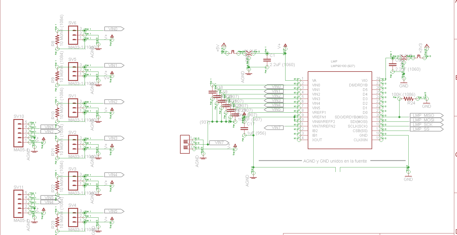
This device features 4-DIFF / 7-SE Inputs (LMP90100/LMP90099). However we saw through data sheet that there would be no drawbacks about using more than four differential channels in our application if we arranged our circuits in order to share one or more common inputs. And that is what we did in the following way:

CH0 = VIN0-VIN7
CH1 = VIN1-VIN7
CH2 = VIN2-VIN7
CH3 = VIN3-VIN7
CH4 = VIN4-VIN7
CH5 = VIN5-VIN7

(VIN6 not used, connected to gnd).
Each sensor is a force load cell made of a double strain gage, configured as a half bridge. We conect them to each of six measuring inputs and use a seventh strain gage on board as a reference. (*) see below more configuration parameters.

Could not upload circuit. Linked image here: drive.google.com/.../view

VREF_SEL = 0 for every channel. This means VREFP1 and VREFN1, which are being connected to sensors power and gnd respectively.

This would allow us to obtain six independent measurements from six half-bridge load cells. Where VIN0 to VIN5 are connected to mid point of those half bridges, and VIN7 is connected to a common reference half bridge. This meets all requirements of a coarse balanced wheatstone bridge in order to work as a substitution/comparison-measurement method.

We have used this configuration for years. And this year we started to employ LMP as a greatly promising sensor AFE, with very convenient advantages respect to its competitors. But unfortunately :( obtained two issues that must be solved:

a) A noticeable cross-talk among channels. That means when a channel goes to rails because of absence of the corresponding sensor (a weak pull up 10Mohm resistor is always present in our circuit), that event modifies values obtained in other channels that do have a sensor plugged in. Besides, when all sensors are present you can see aprox. a 5% cross-sensibility from any channel to others. Today this is patched by software app, but must be improved.


b) Some "noisy" parts. We have manufactured and sold more than one thousand equipments with LMP90100 and noted at QC tests that some LMP devices, about 15% show themselves much more noisy. For those boards the effective number of bits observed falls to 12, when 17 stable bits are expected and used in the 85% of remaining boards. Replacing those apparently-noisy LMP90100 (by "noise-free" devices) through reworking the same pcb, solves this issue. As an experiment, if we lower sample rate from 107 sps to 13 sps or below, noise performance improves greatly and allows 16 or 17 stable bits measures, yet on apparently-noisy devices. I know that low ODRs enhance low pass digital filtering, but why only a portion of ICs are unduly affected?

I think we are missing something important about this device and hope you can provide some help or orientation as we are planning next production.

By the way I hope TI can consider re-writing this great-device's datasheet in order to make it less confusing or less ambiguous about ODR, digital filtering, and adding transparency to background calibration internal operation.

Thanks in advance!

(*)
PWRCN always in active mode
CLK_SEL default, internal clock.
CH_SCAN: Sacan mode 2, First CH0, Last CH5.
CH0 to CH5 CHx_INPUTCN & CHx_CONFIG
Bournout disabled
VREF_SEL = 0, VREFP1 and VREN1
CH0 = VIN0-VIN7
CH1 = VIN1-VIN7
CH2 = VIN2-VIN7
CH3 = VIN3-VIN7
CH4 = VIN4-VIN7
CH5 = VIN5-VIN7
(VIN6 not used, connected to gnd).
ODR_SEL = 0x6, 107 sps
GAIN_SEL = 0x6, 64 with FGA on
BUF_EN = 0.
BGCALCN. BGCALN = 0, off.

  • Belissario,


    Can you please post your schematic in another post? When you start another post, click on "Use rich formatting" and you'll be able to embed images or attach files. Google docs is restricted from the TI internal web, so I can't access your schematic.

    If I have a chance, I'll try to review your posts later tonight.


    Joseph Wu
  • Belissario,


    I checked with the original group that worked on this device and they haven't seen any of the problems that you describe. However, that doesn't mean that there aren't things that we can't look at.

    In for the cross-talk issue, there are two things that I can think of that may affect sampling sequential channels for your measurement. First, if the input is pulled beyond the supplies there may be significant error as the multiplexer fails to correctly sample. If your analog input is 5.5V while the supply voltage is 5V, then you might have this issue. I don't think this is your problem, since it sounds like you're right at the supply voltage. Second, if you have the FGA/PGA enabled and you've over-ranged the PGA, there may be a required time to for the PGA to recover. I don't think there's a way to insert time between channel changes, but you can read from one channel with an over ranged input, and then switch configurations to read from the next channel repeatedly. If the sample recovers to expected value, then this might be the issue.

    For the noise problem, can you give a little more detail about the noise? I'd like to see the raw data (ADC output code for the result). Does this affect all channels or only selected channels? If you were to read from only one channel, do you see the same noise?

    Admittedly, I'm not sure what the problem could be. Generally with Delta-Sigma type devices, the noise performance is well behaved, with little variation from device to device. For your noise change the variation is an order of magnitude. The noise given in Tables 1-4 and in the Typical Characteristics figures are generally going to be consistent.

    When there is noise, I generally check both the reference and the input for excess noise. With your setup, it's less likely to have noise, because you're driving a set of half bridges, where the measurement is ratiometric. Any noise is reflected in both the reference and input, where they should generally cancel. Regardless, I'd check to see if the noise is reduced when the supply is cleaner. If you're using some switching regulator, there might be some interaction with sampling frequency and the switching. The noise may be associated with a specific frequency of operation. Also, if you have any inductance in the supply (as if you're using an LDO as the supply, and a ferrite for filtering), there might be noise in the supply with any digital signals from the ADC. The LdI/dt might cause large spikes in the supply line causing extra noise in the measurement. I would bypass the inductance to see if it helps.

    Again, I'm not entirely sure about the source of your noise, but any information you can give me about it would help.

    Let me know what you think about my comments. Post back with any detailed responses you are able to provide.


    Joseph Wu
  • Dear Joseph:

    Thank you very much for your detailed answer and orientation.

    We have been doing our homework, and this is an update.  About crosstalk issue I think we are going to get over it. For noise problem I am adding new information and tests results. I am writing below between quotes.

    Joseph Wu said:
    Belissario,

    ADC_Dump_CH0_CH1_107SPS_NOISEvsCLEAN.xlsx
    I checked with the original group that worked on this device and they haven't seen any of the problems that you describe. However, that doesn't mean that there aren't things that we can't look at.

    In for the cross-talk issue, there are two things that I can think of that may affect sampling sequential channels for your measurement. First, if the input is pulled beyond the supplies there may be significant error as the multiplexer fails to correctly sample. If your analog input is 5.5V while the supply voltage is 5V, then you might have this issue. I don't think this is your problem, since it sounds like you're right at the supply voltage. Second, if you have the FGA/PGA enabled and you've over-ranged the PGA, there may be a required time to for the PGA to recover. I don't think there's a way to insert time between channel changes, but you can read from one channel with an over ranged input, and then switch configurations to read from the next channel repeatedly. If the sample recovers to expected value, then this might be the issue.

    Checked supply voltage at all QC-failed equipments manufactured last week and always found it ok. Typical value is 5.01V.

    I made lots of tests. Once a sensor is plugged, other channels change measurement as a new steady state. No matter if the input is over ranged.

    One interest test was the following: I have programmed CH5 (VIN4 - VIN7) with a gain of 1 with the intention to not over-range PGA-FGA when a sensor is unplugged. Different from CH0-4 whose gain continues to be 64. Scanmode 2 uses firstCh = CH0, LastCh = CH5. When I plug a sensor at CH5, measurement of other channels loose an average of 3800 counts each (talking in 24 bits). It recovers original meassure when I unplug it.

    I obtained the same results if we program A=64 for CH5 and intentionally over-range it.


    However, as I stated in prior post, this plug/unplug  effect over neighbor inputs can be completely managed by software, but note it does exist, yet taking care to not over-ranging inputs. I included it in this thread because I had the suspect it was related to the noise issue.  Also please note that those pieces going to pass QC ok about noise, are going to present the same plug/unplug effect.

    In regard to that 5% cross sensitivity I could not get to repeat that effect. I cannot be completely sure but we are going to asume it was due to an external issue with probe excitement mechanism. Lets consider there was no such cross sensitivity.

    Then we are going to disregard the complete crosstalk issue.

    About noise

    Joseph Wu said:


    For the noise problem, can you give a little more detail about the noise? I'd like to see the raw data (ADC output code for the result). Does this affect all channels or only selected channels? If you were to read from only one channel, do you see the same noise?

    Yes, you can see the same noise no matter how many channels are selected.

    I have attached a spreadsheet with that raw data. Only CH0 and CH1 were included in the scan in this test in order to get a deeper sample along time, taking maximum advantage from a limited ram space. Any way in the spreadsheet you can see the nature of the noise, wich comes from a kind of "black-lonely-samples". Inside you will also find graphs and a comparison with a typical good device.

    Joseph Wu said:

    Admittedly, I'm not sure what the problem could be. Generally with Delta-Sigma type devices, the noise performance is well behaved, with little variation from device to device. For your noise change the variation is an order of magnitude. The noise given in Tables 1-4 and in the Typical Characteristics figures are generally going to be consistent.

    I think you are right. We obtain the ENOB predicted in those tables for 85% of the devices. And they work fine!

    Joseph Wu said:

    When there is noise, I generally check both the reference and the input for excess noise. With your setup, it's less likely to have noise, because you're driving a set of half bridges, where the measurement is ratiometric. Any noise is reflected in both the reference and input, where they should generally cancel.

    Great! That's our intention too.

    Joseph Wu said:

    Regardless, I'd check to see if the noise is reduced when the supply is cleaner. If you're using some switching regulator, there might be some interaction with sampling frequency and the switching. The noise may be associated with a specific frequency of operation. Also, if you have any inductance in the supply (as if you're using an LDO as the supply, and a ferrite for filtering), there might be noise in the supply with any digital signals from the ADC. The LdI/dt might cause large spikes in the supply line causing extra noise in the measurement. I would bypass the inductance to see if it helps.

    Again, I'm not entirely sure about the source of your noise, but any information you can give me about it would help.

    I have modified some PCBc in order to feed the analog power supply with a 5V linear source, (transformer, full-bridge rectifier, huge electrolitic capacitors, LM7805 regulator, i used to use it at school ;-)  Obtained same results about noise. Failed equipments continue to fail.


    Any way I tested more than eight failed equipments to be sure of results. Normal design uses a step-down buck regulator from TI: TPS62163DSGR. We followed explicit instructions in datasheet about filtering and pcb layout.


    Please bear in mind that when an equipment fails in QC test due to noise, when you replace the LMP90100 part with a brand new one, in general the problem disappears.

    Then I consulted the soldering profiles curves, and they are ok. Lets take in mind that those hand-soldering process (reworking) are always a harsh test for the device.

    If I had to close this today I would conclude that the problem would come from the design/manufacture of the IC. Then we are needing some guide to avoid or get a workaround, for wich we need TI to be explicit about the nature of this noise.

    I will be looking forward for your analysis of that raw data attached.

    Regards.

  • Belissario,


    I started looking through the data plots. Thanks for sending them. My first impression is that there are a few very large excursions of data point error where the output code is several thousand codes off. However, even if you exclude those data points, the resulting data is still noisier than a good board (probably by about 4x of noise). It's hard to tell if the two channels have any correlation between the large noise. There might be some points where the two channels had the same large error, but there's nothing definitive in the error.

    I don't have any conclusions yet. I just have a list of things that you may want to look into.

    1. Normally when I see single point large errors, often they are communications errors. I don't think this is the error in your case because the errors you see are both higher and lower than the typical value (normally, if there's noise on an SCLK line, the SCLK advances the DOUT and makes the data larger). Just to be sure, I would check the communications to see if there is any noise on any of the digital pins.

    2. On boards that fail, I would also check the soldering to make sure the connections are all made. I would use a fine point soldering iron to touch up any connections that look questionable.

    3. Do you remove flux from the boards after completing assembly? In some cases flux is conductive and can cause noise just by conducting signals from other parts of the schematic.

    4. When testing a noisy board, have you tried lowering the gain? Set the gain to 8 and make measurements with the buffer off. I'd like to remove the FGA from the connection to see if there is a problem there.

    5. In the original configuration, can you get a set of data for the inputs shorted to mid supply? If there is noise, I'd like to see if it is additive (for which noise will still appear if the inputs are shorted) or if there is a contribution from the reference (which may not be seen when the inputs are shorted).

    6. AIN7 is connected to a common reference half bridge. What resistances make up that bridge and do you have any capacitance from across the resistors of the bridge?

    7. Out of curiosity, what load cells are you using? I'd just like to know what they are.

    Again, I don't have any conclusions at this time. I'm in the process of getting an evaluation module just to be able to test the device. However, there is a holiday early next week I haven't been able to ask for the board from our normal channel who left a bit early.

    Also I did check with the final test of the device and they do have a cross talk test (in case you still have a problem with that). I didn't see a direct noise test, but they do have multiple integral non linearity (INL) tests that do collect multiple data points and likely store the noise result. At the very minimum, large noise would disrupt the INL test and probably flag that error.

    I'll be on holiday at the beginning of next week. Let me know if any of the comments I've made help you.


    Joseph Wu
  • Joseph Wu:
    Thank you again for your well reasoned answer. I see all your tips are a pretty good guideline.

    You know? We started today to code a filter in order to discard those large-error-samples, and we also realized that resulting data will still be noisier than that obtained in a good board. For each channel standard deviation would lower to 150, but cannot reach 60 or 50 as it is achieved on good boards/devices in a steady state.

    Any way I will perform your suggested tests and update results. I am hopeful and beleive we can, and should, identify the nature of that noise affecting particular parts in order to correct or eliminate it.

    I am not sure I will be able to disclose all the answers in this forum; anyway I agree to update the forum here for general or final conclusions.
    However do you think it might be possible to submit/send full results and answers for TI to be analyzed in a more confidential manner?

    Have a nice holiday!

    Belissario.
  • Joseph Wu

      I have carried out suggested tests and researches. Noise seems to be additive but could not get a conclusion yet.

    Joseph Wu said:


    1. Normally when I see single point large errors, often they are communications errors. I don't think this is the error in your case because the errors you see are both higher and lower than the typical value (normally, if there's noise on an SCLK line, the SCLK advances the DOUT and makes the data larger). Just to be sure, I would check the communications to see if there is any noise on any of the digital pins.

    After examining SCLK and other SPI signals I found neither alteration nor spikes.

    Joseph Wu said:

    2. On boards that fail, I would also check the soldering to make sure the connections are all made. I would use a fine point soldering iron to touch up any connections that look questionable.

    Yes, this was thoroughly checked on all failed boards. No soldering issues were found.

    Joseph Wu said:

    3. Do you remove flux from the boards after completing assembly? In some cases flux is conductive and can cause noise just by conducting signals from other parts of the schematic.

    We don't usually remove it because flux used is a no-clean type embedded in solder past deposited on boards through a stencil print. But I washed some specific boards and tested them. Did not find any changes. Failed boards are very repetitive to continue failing, also good ones continue to pass qc.

    Joseph Wu said:

    4. When testing a noisy board, have you tried lowering the gain? Set the gain to 8 and make measurements with the buffer off. I'd like to remove the FGA from the connection to see if there is a problem there.

    5810.ADC_Dump_CH0_CH1_107SPS_NOISEvsCLEAN.xlsxYes, I exported row data from different experiments in the spreadsheet attached. Please navigate through the tabs to find different changes made respect to the original configuration. Note that on every test I tested one noisy board, one goog board, and in third order I repeated test over the noisy one just to confirm.

    A significant fact is that noise seems to be the same magnitude although gain was divided (not applied) by 16. Standard deviation of the sample (sigma) is an important reference here.

    This test was repeated with that BUF_EN bit both set and cleared. Find results in respective tabs.

    Off topic: BUF_EN = 0 (default) should exclude buffer. But its name results ambiguous. Also if you read datasheet p.54  and observe bad use of terms "exclude in" and "include from" it seems somebody has mixed up BUF_EN description. ;-)

    Joseph Wu said:

    5. In the original configuration, can you get a set of data for the inputs shorted to mid supply? If there is noise, I'd like to see if it is additive (for which noise will still appear if the inputs are shorted) or if there is a contribution from the reference (which may not be seen when the inputs are shorted).

    Yes. Please find results in the respective tab. For this test VIN0, VIN1 and VIN7 were shorted to 2,5V, obtained from a resistive divider derived from 5V applied between VREFP and VREFN.

    Output (aprox zero) enhanced (lowered) noise to the limit for the good board (ENOB tends to 18) but did not improve nor change for the noisy boards.

    Joseph Wu said:

    6. AIN7 is connected to a common reference half bridge. What resistances make up that bridge and do you have any capacitance from across the resistors of the bridge?

    There is a double 350ohm strain gage on-board mounted over a little piece of material equal to that of the load cells. VIN7 is obtained from the midpoint of it.

    We have filter capacitors you can see in the schematic. Under this noise issue those capacitance were put under suspect, were removed and those boards were tested. Obtaining no improvements about noise. 

    Joseph Wu said:

    7. Out of curiosity, what load cells are you using? I'd just like to know what they are.

    They are half bridge load cells.

    Joseph Wu said:

    Again, I don't have any conclusions at this time. I'm in the process of getting an evaluation module just to be able to test the device. However, there is a holiday early next week I haven't been able to ask for the board from our normal channel who left a bit early.

    Also I did check with the final test of the device and they do have a cross talk test (in case you still have a problem with that). I didn't see a direct noise test, but they do have multiple integral non linearity (INL) tests that do collect multiple data points and likely store the noise result. At the very minimum, large noise would disrupt the INL test and probably flag that error.

    I'll be on holiday at the beginning of next week. Let me know if any of the comments I've made help you.

    Joseph Wu

    Fine. I am confident you can contribute with some other orientation & or conclusions.
    Also I hope your are so kind to study those INL tests in search of noise issues records. 
    It seems private messages from e2e platform are not working. I tried to send you one with complementary information but Recipient field on the new message pop-up is not working well (i.e. it rejects your name). Can you contact me by email?
    Thank you.
    Belissario
  • Belissario,


    I see that you're now able to connect with direct messages, so we'll take this offline for the time being.

    I'd note that the device markings that you mentioned are consistent with how we still mark the devices. The devices still have the National Semiconductor logo and the ID code starts with 55 which indicates that it was made in 2015 in May.

    I'm still reading through your data. At this point it does seem that the noise is consistently the same, regardless of gain (as shown by the standard deviation). For gain = 8, I see that the CH0 numbers look correct for the noisy chip, but the gain seems different for the CH1 numbers. Also, the clean chip numbers look like they were taken for a different gain entirely.

    Again, give me some time to go through these numbers.


    Joseph Wu