This thread has been locked.

If you have a related question, please click the "Ask a related question" button in the top right corner. The newly created question will be automatically linked to this question.

ADS5287: Why it can't output always 0 constantly in SINGLE_CUSTOM_PAT test mode

Part Number: ADS5287
Other Parts Discussed in Thread: ADS5294, ADS5282, ADS5281

Dear expert:

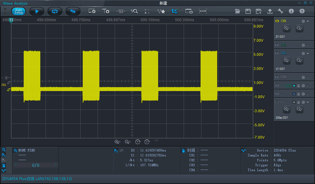
     when we use ADS5287 test mode for SINGLE_CUSTOM_PAT to output all 0 customer pattern. It will have some different data at the output for some times. could you help to explain the reason. please find below test plot. thanks.

Robin

  • Hi,

    What am I supposed to be seeing in that scope plot?  The time scale would seem to indicate that the signal is 'small' for about 0.25ms and large for about 0.1ms.  And by large - almost 7 V?   That would not make sense for an LVDS signal.  What are you programming the SPI registers to be, and how are you using the ADC in your design?   What is your sample clock rate, for example?   I am not seeing much to work with here.

    Regards,

    Richard P.

  • Here we use the FPGA change the LVDS to TTL when they don't have differential probe. But when we use the differential probe have the similar result. The clock frequency is 25Mhz. The register we use lvds test patterns: address 25, 26; for SINGLE_CUSTOM_PAT and set BITS_CUSTOM1[0:9] all zero.

  • After we change the Reset timing. this issue is resolved.

    another question, for the register 46: We need change it to 8110 to get the right SDR output CLKC=12*ADCLK, if set to 8210 as datasheet the CLKC=14*ADCLK.

    After we check ADS5294 as below. 

    So the ADS5287  register 46 table bit: D9 is not match for 10bit setting, could you give some comment. Thanks.

  • Hi,

    So if you write x8110 you get a clock that is 12 * sampleclock?  That would agree with the LVDS Timing Diagram on page 10, since this 10 bit device appends two zeros to the 10 bit data to output 12 bits.  

    The ADS5287 is a 10 bit version of the ADS5281 and ADS5282 device.   So for the 10 bit version of this device the two least significant bits are made zero, but the device still outputs in 12 bit mode.  The ADS5294 is of a different family of devices, but it would not surprise me that some of the Verilog for the digital logic may be common between the two families.   Seeing that in the ADS5287 that the bits D8 through D11 do have an effect on the LVDS clock output would confirm this.     The datasheet for the ADS5281 and ADS5282 say to always write '1' to bit D9 which would be correct for those devices.    It may be that for the 10bit ADS5287 that it would be D8 that should get a '1' instead of D9, but I would have to confirm that with the design team.  Since the 10 bit device makes the two lsb's zero, it may be that the clock rate is lengthened by two bits so that selecting '10bit' operation means the output clock is 12x, and '12bit operation' would result in a clock 14x, etc.    But looking at the datasheet for ADS5294 is only a clue as to why you see what you see, since that is a different device.  I will ask the design team for confirmation.  But in the meantime write x8110 if that gives you the operation you wish to see. 

    Regards,

    Richard P.