This thread has been locked.

If you have a related question, please click the "Ask a related question" button in the top right corner. The newly created question will be automatically linked to this question.

ADS1292: SPI communication

Part Number: ADS1292

First time using the part and have SPI questions. Using a Microchip controller and set CKE and CPOL to 0  - SCLK is running at 500khz.

The chip responds to 8 bit commands  -  writeSPI4(0x08);  //start conversions - ~DRDY active *see the pin going low

                                                                 writeSPI4(0x06);  // ~DRDY inactive *see all pins going to reset state

I have a BEAGLE SPI analyzer see activity on MISO on 8 bit above transfer.....didn't expect it.

Also, set up read register protocol as directed but data read is garbage. Am I missing a relationship between setting a function using a pin or SPI command?

Thanks


  • Hi Joe,

    Thanks for evaluating our ADS1292!

    The SPI settings you should be using are CPOL = 0 AND CPHA = 1, which means SCLK will idle low, data will shift on the rising edge, and data will latch on the falling edge. I'm not sure what "CKE" means - could you clarify that?

    Are you sending the SDATAC command first before any other commands? This is needed to exit RDATAC (Read Data Continuous) mode, which is the default, before other commands can be properly recognized.

    Best Regards,
  • Thanks Ryan, that resolved my first issue. Second issue is when I issue the RDATA command I don't get status back. Any thoughts

    Joe
  • Hi Joe,

    Are you sending enough clocks? STATUS + Channel data will only appear after the RDATA command is decoded on the 8th SCLK falling edge. Also, is the ADC converting? Either the START pin should be pulled high, or the START command must be sent if the START pin is low. /DRDY will pulse at the data rate when the ADC is actively converting.

    Best Regards,
  • Hi Ryan,

    I've changed my code to implement the RDATAC usage on page 36 of the data sheet. I've attached a file with the Beagle
    SPI capture. When I turn on my ECG simulator as input to IN2 And IN1 I see no change. Any thoughts? All clocks and timing look
    good even getting 0xC0 Status back on MISO. Please notify me if the file did not upload properly.

    Thanks,

    Joe

  • Hi Joe,

    The Beagle SPI capture file did not upload.

    Since you are seeing the beginning of the STATUS word, the device must be converting properly now. Can you configure Channel 1 for the internal test signal and plot the data? The test signal amplitude and frequency are configured in the CONFIG2 register. You'll also need to write CH1SET[3:0] = 0101.

    Best Regards,
  • ADS1292 Characterization.docxRyan,

    I have attached the file again.  I hope the Beagle Capture data will give you some insight.

    Thanks,

    Joe

  • ADS1292Schematic.pdfRyan, Attached is the schematic the hardware designer gave me. He said he got it from a eval. kit. I apologize for it's appearance.

  • Hi Joe,

    Thanks for the updates. I looked through the characterization document. Channel 1 is definitely saturated, while Channel 2 seems to show some noise at least; however, if you say that all inputs are grounded, then there is quite a bit more noise than I would have expected.

    Can you please share the complete register settings for the device? Did you try configuring either channel to use the internal square wave test signal? There's an example of how to do that at the bottom of Figure 63 in the datasheet.

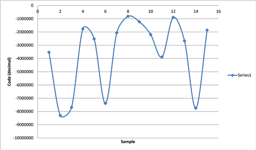
    Your data (lines 46 - 88):

    Code (Hex) (Code) Decimal
    ca1053 -3534765
    814c49 -8303543
    8ab8c2 -7685950
    e5109b -1765221
    d97fad -2523219
    8F3d8a -7389814
    e07cfe -2065154
    f39963 -812701
    ed3bf6 -1229834
    de8c1c -2192356
    c4a85c -3889060
    f24aed -898323
    d72c58 -2675624
    89b579 -7752327
    e39968

    -1861272

    Best Regards,

  • Hi Ryan,

    Could you see attached and comment?

    Thanks,

    JoeADS1292 questions.docx

  • Hi Joe,

    The structure for the RREG and WREG commands calls for the number of registers to read / write minus one. Therefore, to read from / write to two registers, the second byte in the SPI command will be 0x01. You are sending 0x02 as your second byte (meaning you wish to read / write three registers), but you're only sending enough SCLKs for two registers. Hope that clarifies the command structure.

    The test signal appears to be configured properly for channel one and 0x0049F2 is in the correct range. For VREF = 2.42 V and Gain = 6, the LSB size is equal to 48.081 nV (see equation below). Therefore, 0x0049F2 (18930d) equates to 0.9102 mV. The expected amplitude of the square wave test signal is 1 mV.

    1 LSB = [2*VREF / Gain / 2^24] = 48.081 nV

    18930 * 48.081 nV = 0.9102 mV

    Best Regards,

  • Hi Ryan,

    Your help is greatly appreciated.

    Thanks,
    Joe