This thread has been locked.

If you have a related question, please click the "Ask a related question" button in the top right corner. The newly created question will be automatically linked to this question.

[FAQ] ADS1282: Data formatting & LSB Size

Part Number: ADS1282

Hi all,

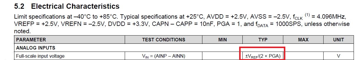
For unipolar mode (AVDD=5V, AVSS=0V, VREFP=5V, VREFN=0V), ADS1282 full-scale input voltage is from 0V to 2.5V. Am i right?

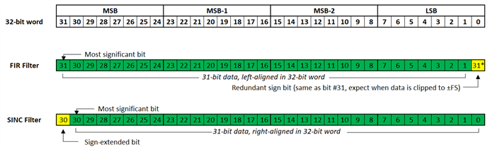
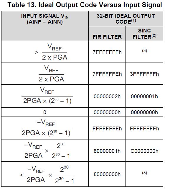
Also data code is range from 00000000h to 7FFFFFFFh for FIR filter. Am i right?

Most of data in the datasheet is according to unipolar mode. Thus, i'm not sure about this subject.

Regards,

Eren

  • Sorry for mistake. *most of data in the datasheet is according to bipolar mode

  • Hi Eren,

    The difference in data formatting for FIR vs SINC filter mode is a little confusing, let me try to clarify...

    First off, the supply mode (unipolar or bipolar) will have no effect on the data format. However, how you configure the supplies will affect the ADC's common-mode input range. In other words, the AVDD and AVSS supply voltages will put a restriction on the absolute voltages that can be applied to the analog input pins.

    The output data is not related to the absolute input voltages, but rather the differential voltage between AINP and AINN. The maximum differential voltage that can be measured by the ADC is +/- (Vref / [2 * PGA]). Therefore, for a 5V reference and PGA = 1 V/V, the ADS1282 can measure differential inputs within +/- (5V / [2 * 1V/V]) = +/- 2.5V.


    Where things get to be confusing is the difference between FIR filter mode and SINC filter mode. In both modes you'll clock out a 32-bit word and get 31-bit, two's complement signed-data, however here is the difference...


    • In FIR filter mode, the 31-bit data is LEFT-ALIGNED in the 32-bit word and the least significant bit is a redundant sign bit (expect when the output is clipped to +/- FS)....

      Positive voltages (between 0 and +FS, +2.5V for this example) will have output codes ranging from 0000 0000h to 7FFF FFFEh; while negative voltages (between 0 and -FS, -2.5V for this example) will have output codes ranging from FFFF FFFFh to 8000 0001h. When the differential voltage exceeds the +FS or -FS voltage the LSB will flip, so positive voltages exceeding +FS will result in an output code of 7FFF FFFFh and negative voltage exceeding -FS will result in an output code of 8000 0000h.
       
       
    • In SINC filter mode, the 31-bit data is RIGHT-ALIGNED in the 32-bit word but the data is already sign-extended...

      Positive voltages (between 0 and 2.5V) will have output codes ranging from 0000 0000h to 3FFF FFFFh; while negative voltages (between 0 and -2.5V) will have output codes ranging from FFFF FFFFh to C000 0000h. When input voltages exceed +FS or -FS, you will notice that the output codes will not clip to 3FFF FFFFh or C000 0000h, but will continue to increase.
       

    NOTE: At the fastest SINC filter data rates you may only have enough time to clock out 16- out of the total 32-bits of data, so you will need to stop clocking out data after the first two bytes.

    I hope that explanation helps. Let me know if you have any additional questions!

    Best regards,
    Chris

  • Hi Chris,

    Thanks a lot for the help.

    Regards,

    Eren