This thread has been locked.

If you have a related question, please click the "Ask a related question" button in the top right corner. The newly created question will be automatically linked to this question.

ADS1259-Q1: Data output stops, restarts after reinitialization

Part Number: ADS1259-Q1
Other Parts Discussed in Thread: MSP430F2619, ADS1259

I'm currently working on a tool that includes an ADS1259-q1 and msp430f2619 mcu. The ADS is taking 1 conversion/ms for 1 sec every 300ms. The chip is setup below and gives expected readings for the first  3-7 conversion periods* when tested with 2Vpp sine wave. After that, it stops sending data. After I reinitialize the ADS every other conversion period, data output resumes, but still skips 1-3 conversion periods before resuming.

Stepping through the code in CCS doesn't reproduce the issue. I noticed it while letting the program run while watching the DOUT ADS pin on oscilloscope. I'm not sure what the issue could be. This is my first post here, so let me know if I need to include anything else. Thank you for your time.

*Conversion period = the 1 sec where ADS takes 1 conversion/ms

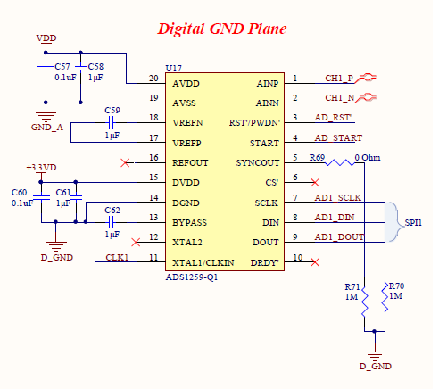
MCU uses 16MHz external clock, The ADS SCLK uses SPI clock set to 2 MHz

----------------------------------------------------------------------

ADS Initialization/reinitialization Procedure:

Set RST pin (on ADS) low, then high again

wait 10 ms

SDATAC (0x11)

WREG from address 0h for 6 registers

CONFIG0 = 0x05 (default settings)

CONFIG1 = 0x00 (no external ref, all other settings default)

CONFIG2 = 0x17 (Pulse Control mode @ 14.4K SPS)

Offset registers set to 0x7fffff

RDATAC (0x10)

--------------------------------------------------------

ADS reading procedure:


for (index = 1ms; index < 1000ms; index++){

while (timer < index){

START ADS pin = high

wait 4 clock cycles

Start = low

wait 0.5 ms

UCA0TXBUF = 0x00 to request 8 bits of reading from ADS. SPI interrupt receives and processes

Repeat previous step two more times for full 24-bit reading.

}}

  • Hi Michael,

    Welcome to the TI E2E Forums!

    From your schematic, I noticed that the /CS and /DRDY pins are floating...

    - Floating the /CS is a problem since the device will only respond to commands when the /CS pin is low. If this pin were to float to a high logic state, then the device would stop responding. This might explain the behavior you're seeing. I usually recommend controlling this pin via a GPIO; however, if that is not an option then this pin should be tied low (resistor to DGND).

    ALSO NOTE: "D_GND" and "A_GND" should be connected together somewhere in your circuit; preferably right at the ADC.


    - Floating the /DRDY pin is not an issue since this is an output signal; however, with out this "data ready" indicator to use as an interrupt you might run into the issue where you are reading old data, or perhaps even reading corrupted data (if you happen to be reading data while a conversion completes, which provides you with a mix of old + new data). Since you are floating this pin, I would recommend putting the device into "Stop Continuous" mode (using the SDATAC command) and polling bit 7 in the CONFIG2 register to realize when new is available. Once new data is available, I would then read the conversion result with the RDATA command (while still in "Stop Continuous" mode).

    Keep in mind that a polling implementation of /DRDY may require you to at least poll 2-4x times faster than the data rate (that's just my rule of thumb) to ensure that you don't lose any data.
     

    I hope that helps!

    Best regards,
    Chris

  • Sorry for not getting back to you sooner.

    After connecting the grounds and grounding chip select, I haven't noticed any change in the behavior. However, I have noticed that there is a change in VREFN and VREFP when I lose data.

    Below, yellow represents the DOUT pin and blue is the VREFN pin

    Something similar happens at VREFP (in blue), but not to the same degree.

    I'm still looking over the rest of the system to make sure there isn't something else in the system that would cause this.

  • Hi Michael,

    That is a very interesting observation! It makes me thing that the internal reference is not working properly.

    • I would double check that the EXTREF register bit is not set in order to use the ADS1259's internal reference source.
    • Additionally, I also see that the REFOUT pin is missing a 1uF capacitor, used to stabilize the internal reference. Try adding a 1uF cap between REFOUT and AVSS.


    See if either of the two suggestions above stabilize the voltage on the VREFN pin...

    Best regards,
    Chris

  • Adding the cap hasn't changed the issue either. However, reading the registers back, I noticed that CONFIG2 isn't set to my specs. When I read back, I get

    CONFIG0 = 0x25 (factory bits + default)
    CONFIG1 = 0x00 (no extern ref)
    CONFIG2 = 0x00 (default)

    In case I'm doing something wrong in writing to ADS, my code is as follows.

    writing to registers:
    ---------------------------------------------------------------------------------------------------
    UCA0TXBUF = 0x11; //SDATAC
    while (!(IFG2 & UCA0TXIFG)); //wait for TXBUF to be empty

    UCA0TXBUF = 0x40; //WREG command - from address 0h
    while (!(IFG2 & UCA0TXIFG));

    UCA0TXBUF = 0x06; //WREG command - 6 registers
    while (!(IFG2 & UCA0TXIFG));

    UCA0TXBUF = 0x05; //CONFIG0
    while (!(IFG2 & UCA0TXIFG));

    UCA0TXBUF = 0x00; //CONFIG1
    while (!(IFG2 & UCA0TXIFG));

    UCA0TXBUF = 0x17; //CONFIG2
    while (!(IFG2 & UCA0TXIFG));

    UCA0TXBUF = 0xff; //offset
    while (!(IFG2 & UCA0TXIFG));
    UCA0TXBUF = 0xff;
    while (!(IFG2 & UCA0TXIFG));
    UCA0TXBUF = 0x7f;
    while (!(IFG2 & UCA0TXIFG));

    UCA0TXBUF = 0x10; //RDATAC
    while (!(IFG2 & UCA0TXIFG));
    --------------------------------------------------------------------------------------------------------

    reading register settings:
    ---------------------------------------------------------------------------------------------------------
    UCA0TXBUF = 0x11; //SDATAC
    while (!(IFG2 & UCA0TXIFG));


    UCA0TXBUF = 0x20; //RREG command - from address 0h
    while (!(IFG2 & UCA0TXIFG));

    UCA0TXBUF = 0x02; //RREG command - 3 registers
    while (!(IFG2 & UCA0TXIFG));

    UCA0TXBUF = 0x00; //read CONFIG0
    while (!(IFG2 & UCA0TXIFG));

    UCA0TXBUF = 0x00; //read CONFIG1
    while (!(IFG2 & UCA0TXIFG));

    UCA0TXBUF = 0x00; //read CONFIG2
    while (!(IFG2 & UCA0TXIFG));

    UCA0TXBUF = 0x10; //RDATAC
    while (!(IFG2 & UCA0TXIFG));
  • Hi Michael,

    Michael Green69 said:
    UCA0TXBUF = 0x06; //WREG command - 6 registers
    while (!(IFG2 & UCA0TXIFG));

    I noticed a minor bug here..."0x06" will tell the device that you are going to write to 7 registers. Therefore, the "0x10" (RDATAC) command may actually be interpreted as a write to the FSC0 register. I don't think this is the cause of your problem though.

    It is also a bit odd that you're reading a value of "0x25" for the CONFIG0 register...If the ID bits are "10b", then you should be reading a value of "0xA5" since bit 7 of the CONFIG0 register always returns a 1. This make me wonder if there might be other issues with the SPI communication...

    • What frequency are you using for the ADC's master clock...are you applying an external clock signal to the CLKIN pin or are you grounding this pin and using the internal oscillator? With a 2 MHz SCLK, any external clock must between 3.6 and 8 MHz. 

    • Is your SPI configured to communicate using SPI mode 1 (CPOL = 0; CPHA = 1)? If not, you could be reading and writing slightly different values than what you're expecting.

    • Have you looked at the SPI signals on the oscilloscope to see if they are clean (free from glitches and large overshoots)?

    Best regards,
    Chris

  • Hi Michael,

    Where you able to resolve this issue? Please let me know if you need any additional assistance!

    Best regards,
    Chris
  • Sorry about not replying. As it turns out, my analog and digital grounds were not meeting as I thought. I will continue to monitor the SPI, but your original suggestion on grounding solved my issue. Thank you very much.