This thread has been locked.

If you have a related question, please click the "Ask a related question" button in the top right corner. The newly created question will be automatically linked to this question.

ADS1015EVM: Noisy READY line does not reach GND

Part Number: ADS1015EVM

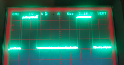
Debugging some strangeness in conversions, I decided to implement the ADS1015 ALERT/RDY line for an interrupt-driven method of reading the results register in both auto and manual conversion mode.

I have set the config register, bits 0 to 4, to 0x03, per the data sheet.  This is expected to provide an active low signal when a conversion is complete.

I am using the ADS1015EVM (Rev C) board in my test hardware.

Examining this line on a scope caused some concern.

This happens with both ADS1015's and on both READY/ALERT lines.

I have two ADS1015EVM boards, so swapped in another one.  Same result.


I replaced one of the ADS1015 ADC's.  No change.

I removed Q1A/B.  No change.

This is quite perplexing.  I see the same ragged crappy signal on both sides of the non-inverting buffer, U5.


Here's a snip of my ADS1015EVM schematic:


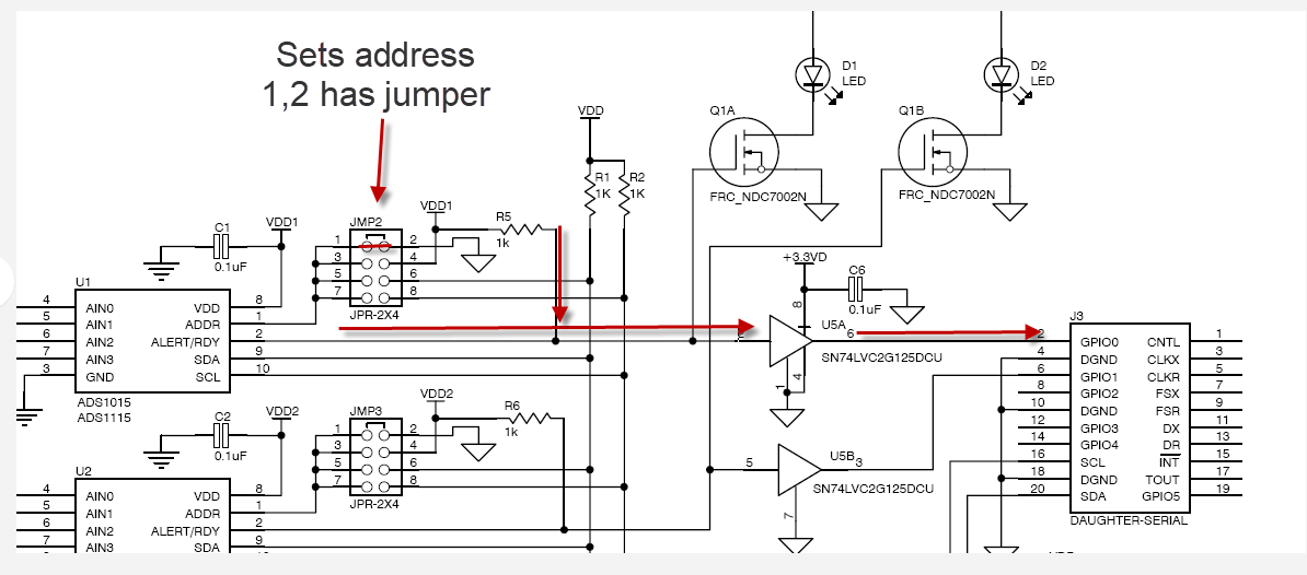
This is rather late in the game for our development commitment to this device.  So would be good to know, ASAP, if we can use READY/ALERT on this chip.  At the moment, this seems unlikely.


  • Hi k1mgy,

    There are a couple of things we need to verify, but for the Alert pin to signal the end of conversion both the Configuration register and the Hi and Lo threshold registers need to be set correctly.

    For the Configuration register, lets take a look at the bit 4 through bit 0.

    • Bit 4 is Comparator mode and can be set to either mode as the threshold registers will be set to always exceed the value and thus trigger an alert
    • Bit 3 selects whether the alert output is active high or active low an can be left at the default setting
    • Bit 2 can be set to the latching state where it will stay in the activated state until the device is read
    • Bits 1:0 sets the state of the alert function the number of conversions before the alert takes place.  These bits must not be '11'.

    You stated you are using 0x03 which disables the comparator.  It would be better to use 0x00.

    Also, section 8.3.8 in the ADS1015 datasheet discusses the comparator threshold settings.  Basically you need to set the threshold settings so that the comparator is always triggered.  Set the MSB of the Hi threshold registers to 1 and the MSB of the Lo threshold register to 0.

    Also, make sure you have a good ground connection from the EVM to your controller.

    Best regards,

    Bob B

  • Yes, I have good grounds. However I am NOT supplying +3.3V at J2. Only +5V. If I supply +3.3V the ratty pulses go away and I get nothing on ALERT/RDY.

    It appears that the +3.3 is needed for the level shifting. However, my TWi works fine without it...

    I was under the impression that the comparator should be disabled. But "Assert after one conversion", etc might have offered me a clue, had I read it more carefully!

    I'll give that a try and report back here the results.
  • Hi k1mgy,

    The level shifting is needed for the PDK version we had of the ADS1015 as the motherboard (MMB3) is 3.3V only. You should be able to jumper pins 9 and 10 on J2 and all should be happy for the whole board. 3.3V is not a requirement unless using the MMB3 motherboard. However it is best to power the unpowered devices on the EVM.

    Best regards,
    Bob B
  • Bob B, thank you for the quick and VERY helpful reply.

    My host runs on 3.3v logic, so I must rely on the level shifters aboard the EVM.

    So, I've applied +3.3V. There's no READY signal now. However, I'm not complete with changes to the configuration. About to set up the comparator.... As they say, "film at 11".

    So, we'll soon see if this does the trick.
  • Was hoping your instructions would solve the issue.  Guess it's not going to be so easy :)

    Here's the I2C traffic for the full configuration.

    The first frame sets up the ADC as desired.  The second sets the low comparator register to 0 and the third sets the high comparator to 0x8000 (msb==1)

    In continuous or single-conversion mode, the ALERT/RDY line still stays high (at +3.3V)

    As I noted, when NO +3.3V was applied to J2, I saw these pulses, but they were very ragged and did not reach GND.  What's strange is that I had not set up the comparator as you suggest and saw these pulses.  So not certain what's (still) going on.

    Note that the original problem I'm looking into is frequent bad data.  It's intermittent...  Testing an integrator with a steadily-rising output, I often see a measurement that is lower than the previous measurement.  I figured that perhaps the conversion register was being updated at the moment it was being read.. and perhaps triggering a read on the ALERT/RDY line would be a safer bet.

    Which raises the question: the data sheet says that the conversion register may be read at any time.  Even in continuous conversion mode?  

  • Hi k1mgy,

    Note the data for writing the register pointers for the high and low threshold is incorrect. Low should be 0x02 and high should be 0x03.

    As far as reading the conversion registers, it is best to avoid the conversion update period (8us) that is illustrated in Figure 14. Depending on data rate and I2C clock speeds most likely this will never be an issue, however I prefer using the Alert/Ready signal as an interrupt to make sure that never catch the update region just in case.

    Best regards,
    Bob B
  • That did it.
    I now have perfect ready pulses.

    Can't thank you enough.

    I intend to write up a brief paper that will help others like me (who need a quick reference) to be successful with this converter.

    Are you working for TI?  If not, they need you :)

    /m