This thread has been locked.

If you have a related question, please click the "Ask a related question" button in the top right corner. The newly created question will be automatically linked to this question.

ADC32RF45EVM: Operational Issue

Part Number: ADC32RF45EVM
Other Parts Discussed in Thread: ADC32RF45, ADS54J42, LMX2582

I have a customer using the ADC32RF45EVM in his application. He explains his issue below:

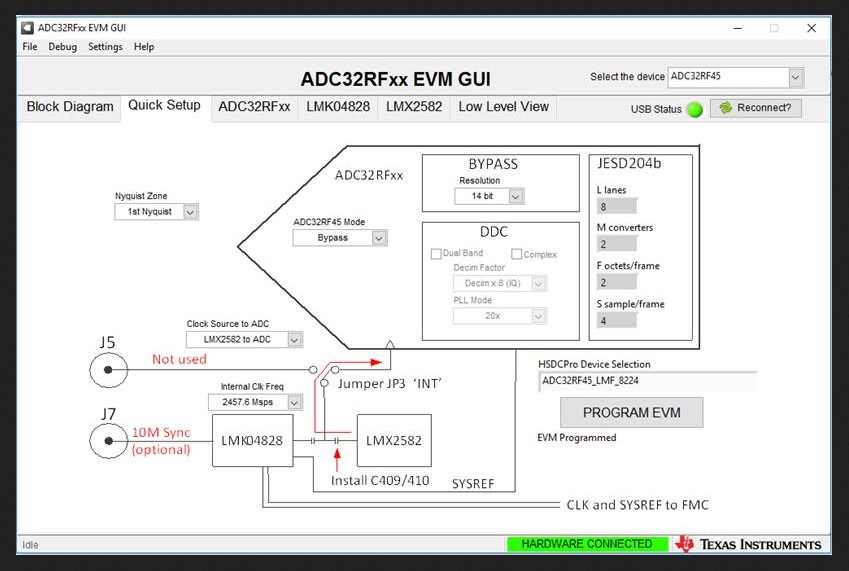
I am using the Xilinx KCU105 with the ADC32RF45EVM. I am following the instructions in the "HSDC Pro with Xilinx KCU105.pdf" document. But when it gets to the board setup example (Section 7.3) it only has an example using an external clock. I do not have an external clock available. I have tried to configure it for an internal clock, but I continue to get errors. My board has C409/410 installed, not C431/432.

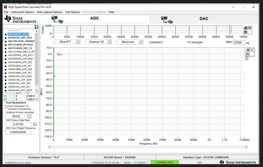
I have tried using various configuration files you provide, but none seem to work. When I put it in time domain and hit "Capture", I get "Configure ADC CMD_EXEC_ERROR when control command fails". If I click "OK" and try again, I get "Read DDR to file TIMED_OUT_ERROR Time Out error"

Do you know what might be happening here? Is this just a software issue? I thought that it might, but the inability to reconfigure the clock made me think that this might be related to something else.

Please let me know if you have seen this issue before and if you might have a solution.

Thanks for your help with this!

Richard Elmquist

  • Hi Richard,

    We are looking at your question and will response back soon.

    Regards,
    Neeraj
  • Hi Richard,

    We are looking at your question and will get back to you soon.

    Regards,
    Neeraj
  • Neeraj,
    What the customer is looking for is the following:
    "What I need is an example project that uses the internal clock instead of the external clock. If I could go through an example using configuration files that are known to work together (There are two and I don’t know which pairs are compatible for my board with C409/410 installed), then I could confirm whether I really have aq problem or if I just have not configured the device properly."
    Thanks for your help with this!
    Richard Elmquist
  • Richard,

    Have the customer follow the attached example. This currently works with the TSW14J56EVM. For the case when using this with the KCU105, they may have to change a clock divider setting in the LMK output clock tab. Make sure they move C431 and C432 to C409 and C410. This is on the bottom of the board near the LMX device. They also need to move the shunt on JP3 to pins 1-2 (INT). This setup will have the ADC sampling at 2.4576Gsps.

    Regards,

    Jim 

    ADC32RF45_Bypass_Int_Clk.pptx

  • Jim,
    Thanks so much for your help!
    I will let you know if the customer has any further questions.
    Have a great day!
    Richard Elmquist
  • Jim,

    The customer has come back with a further response. I do not know if we can help him but here it is:

    On my version of High Speed Data Converter Pro v4.80, it is not possible to set up the Quick Setup as shown in the power point you sent me. The reason is that my choices in the ADC Select box only has one option for the ADC32RF45. You want me to select ADC32RF45_LMF_8224. But my only choice in the drop down list is ADC32RF45_42810, which doesn’t work. 

    I tried to update the GUI software, but it says it is already up to date. How do I get more than one choice for ADC32RF45 configurations so I can select the one you suggest? (There are several choices each for other ADCs in the drop down list)

    I have attached some screen shots so you can see what I’m doing.  The first picture shows my settings in the EVM GUI.  You can see that this exactly matches the Quick Setup Tab settings that were in the power point you sent me. 

    The second picture shows the HSDC Pro screen where I am trying to select the correct ADC configuration from the drop down list.  You can see many options for other ADCs but only the one I have selected for the ADC32RF45, which as I pointed out, does not work for the settings in the EVM GUI.

    I hooked up my 32RF45EVM board to a TSW14J56 board and configured as shown in the power point presentation and it works just fine.  I have lots of choices for selecting the ADC, including the one shown: ADC32RF45_LMF_8224.  The problem is that when I hook it up to the KCU105, I only have one ADC option: ADC32RF45_42810. 

    I either need updated firmware that will allow me to select other device options, or I need instructions on how to configure the device for ADC32RF45_42810 using an internal clock.

     The fact that there are no other options available for the KCU105, makes me wonder if anyone has ever used the KCU105 with the ADC32RF45EVM in internal clock mode before.

    I do not know if we can help him. Is there anything we can offer?

    Thanks for your help with this!

    Richard Elmquist

  • Richard,

    I am working on getting my KCU105 setup running but not there yet. I did find an ini file that the customer needs, but I am unable to verify it until I get my system running. You can pass this on to him to see if it works. Have him place it in the following directory: 

    C:\Program files(86)\Texas Instruments\High Speed Data Converter Pro\KCU105 Details\ADC files

    Regards,

    Jim

    https://e2e.ti.com/cfs-file/__key/communityserver-discussions-components-files/73/ADC32RF45_5F00_8224.ini

  • Jim,
    Thanks for your help!
    I will let you know what happens.
    Have a great day!
    Richard Elmquist
  • ADC32RF45__LMFS_8224_Int_Clk_KCU105.pptxRichard,

    I was able to get my system up and running and verified this ini does work. There is one setting the customer will have to change in the LMK output clock section. See attached start up guide.

    Regards,

    Jim

  • Jim,
    Thanks so much for your hard work!
    Have a great day!
    Richard Elmquist
  • Jim,

    They are still having issues.

    I have attached a Word document that explains the issue.

    ADC32RF45 Issue at GFI Engineering.docx

    Do you want to work directly with the customer? Let me know.

    Thanks for your help with this!

    Richard Elmquist

  • Jim,
    Have you had a chance to look at the document I sent in the previous post?
    Please let me know if you have any further questions or options for the customer.
    Thanks for your help with this!
    Richard Elmquist
  • Richard,

    Can you verify the customer moved the caps to C409 and C410 on the ADC EVM? Also in HSDC Pro GUI, have them click on the "Capture Options" tab at the top of the GUI, then select "Capture Options", then set the # samples (per channel) to 32,768.

    Regards,

    Jim

  • Jim,
    Thanks!
    I will let you know if the customer has ant further questions.
    Have a great day!
    Richard Elmquist
  • Jim,

    The customer has the board working but is still seeing issues:

    I have mostly good news.  I am now able to capture data on the ADC.  However, I still get the DDR timeout error intermittently.  I found that when I connect to a 1G Ethernet, it does not capture very often.  In 10 tries, it will give the DDR error 9 times (I have to disconnect and reconnect between tries).  However, if I connect over 100Mbit Ethernet, it works most of the time.  When I get the DDR error, I disconnect from the board and reconnect.  That usually fixes it. 

     Do you have any suggestions for getting a more reliable connection?  We need 1G Ethernet for our application.

    Now that I have it working (at least intermittently) can you tell me what changes I need to make to run it at near 3G samples per second? I tried just changing the frequency to 3.072G in the ADC32RFxx EVM GUI and the HSDC Pro software, but I get a configuration error in the HSDC Pro software.

    Here is another interesting fact.  When I select ADC32RF45_42810 (even though the device is configured in 8224 mode), the capture button works every time.  It never fails.  As soon as I switch back to 8224 mode, it becomes intermittent again.  Once it fails, it will never succeed without either disconnecting and reconnecting, or selecting 42810 mode and then switching back. This only works sometimes. 

    After doing more testing, I am still not able to capture data reliably.  Here is what is happening:

    1.       If I follow all of the instructions given by the engineer, the first time I click the “Capture” button, I can successfully capture data.

    2.       If I then click the “Capture” button again, I get the “Read DDR to file TIMED_OUT_ERROR”.  Once this occurs, it doesn’t matter how many times I click “Capture” the error repeats and cannot recover.

    3.       If I disconnect from the KCU105 and reconnect, it will again capture data the first time but then gets the DDR error on all subsequent attempts to capture data.

    4.       If I switch the ADC device from ADC32RF45_8224 to ADC32RF45_42810 (Even though I know this is not the configuration of my device), I can capture data successfully all of the time.  I have seen the DDR error a couple of times in this mode, but once it starts capturing, it seems to remain reliable from then on.  However, the few times I did see the DDR error, just like the _8224 case, it is permanently broken and never recovers without a disconnect/reconnect.

    Until I can get reliable capturing of data at about 3GS/s, I cannot use this ADC.  As I mentioned before, my KCU105 works great with the ADS54J42 so I know it is not a KCU105 problem.  Also my ADC32RF45 board works great on the TI TSW14J56 EVM so I know there is nothing wrong with my ADC board.  It is only the combination of the ADC32RF45 EVM with the KCU105 that will not work.  Hopefully, the information I provided above will give the engineer some clues as to how to get around this problem.

    I do not know how to address the customers questions.

    Would you like to work directly with him to try and solve these issues? Please let me know via email if this is the way you want to go and I can provide the customers information.

    Thanks for your help with this!

    Richard Elmquist

  • Jim,
    Have you been able to look at these further questions from the customer?
    Please let me know if you can offer some options for the customer.
    Would it be better if you were to work directly with him?
    Thanks for your help with this!
    Richard Elmquist
  • Richard,

    The KCU105 appears to struggle when operating with a serdes lane rate above 8GHz. We have been working with Xilinx on getting this fixed. This is a low priority for the team at Xilinx and not sure when we will get something back from them, as they designed this firmware. The issue may be related with the interface with HSDC Pro. Xilinx does have example code that does not use HSDC Pro and is available on their website. You may suggest to the customer to give this a try.

    Regards,

    Jim 

  • Jim,
    Thanks for your response!
    Have a wonderful holiday.
    Richard Elmquist
  • Jim,

    The customer sent me the following response:

    We have decided to order the Xilinx VC707 board and the TSW14J10EVM.  We would like to use the exact same setup your engineer used to get this working with the ADC32RF45EVM at 2.31Gsps.  Can you please provide us with any configuration files we will need as well as a description of the procedure we need to use to get the system working?  We would also like to look at the possibility of running at a higher sample rate (and same serdes frequency) by reducing resolution from 14 to 12 bits.  Could you also provide the configuration for that mode?

    Can we offer him any help with this?

    Do you think that you might want to work directly with the customer to speed this up? Let me know.

    Thanks for your help with this!

    Richard Elmquist

  • ADC32RF45_8224_VC707_2.2G_Fs.pptxRichard,

    I just got off the phone with Xilinx and it appears the serdes on the VC707 is only rated up to 10.3GHz due to the speed grade they use for this board. I am able to push this to 11.25Gbps with our board, but there is no guarantee this will always work. I have attached the start up guide I used for this. Xilinx did mention both the KCU105 and ZCU102 have parts that will run up to 12.5Gbps, but we are still struggling to get this work at this rate. We are working with them on this, but not sure when this will get resolved.

    Regards,

    Jim

  • ADC32RF45_82820_VC707_2.8G_Fs.pptxRichard,

    Attached is an example running the ADC in 12 bit mode sampling at 2.GHz and capturing the data with a VC707.

    Regards,

    Jim

  • Jim,
    Thanks for your hard work on this.
    I will send this information to the customer.
    I will let you know if they have any additional questions.
    Thanks for your help with this!
    Richard Elmquist
  • Jim,

    The customer has several other questions:

    We are required to use the internal clock – not an external clock. Can the engineer modify his instructions to use the internal LMX2582 as the clock source?

    What is the purpose of the interposer card between the ADC Eval board and the VC707?

    What do you use as your source for the external 2.2GHz clock? Is there a manufacturer/model number we should get?

    I have the instructions, but I cannot find the code to load on the VC707 for this demo. Please provide the link ASAP. I’m ready to start testing.

    In the HDSC Pro Gui, the ADC32RF45 modes available when selecting the ADC are 8224 and 42810.  But for 12-bit operation, we need 82820 mode.  Can you please provide the ADC32RF45_82820.ini file for the KCU105?

    Can you help with these questions?

    Thanks so much for all your help!

    Richard Elmquist

  • Richard,

    Answers below

    We are required to use the internal clock – not an external clock. Can the engineer modify his instructions to use the internal LMX2582 as the clock source?

    Move JP3 to pins 1-2

    What is the purpose of the interposer card between the ADC Eval board and the VC707?

    This allows HSDC Pro GUI to load the FPGA firmware and read and write from the FPGA using the USB port on the interposer board.

    What do you use as your source for the external 2.2GHz clock? Is there a manufacturer/model number we should get?

    We use a Rhode & Schwarz SMA 100 signal generator.

    I have the instructions, but I cannot find the code to load on the VC707 for this demo. Please provide the link ASAP. I’m ready to start testing.

    In the HDSC Pro Gui, the ADC32RF45 modes available when selecting the ADC are 8224 and 42810.  But for 12-bit operation, we need 82820 mode.  Can you please provide the ADC32RF45_82820.ini file for the KCU105?

    ini attached.

    Regards,

    Jim

    https://e2e.ti.com/cfs-file/__key/communityserver-discussions-components-files/73/ADC32RF45_5F00_82820.ini

  • Jim,
    Thanks for your help.
    I hope that you have a wonderful weekend!
    Richard Elmquist
  • Jim,

    I am not sure how to answer the customer. This issue is way beyond my knowledge as I am not familiar with the code. Here are some of his comments. The logs that he is referring to were so small I could not read them. I will send them once he resends them to me:

    To help you understand better what is going on, I have attached snippets of the HSDC Pro status log for a successful capture of data and when it fails. 

    Here is what the log looks like when I hit the Capture button and the data is successfully displayed on the HSDC Pro Gui:

     When it fails, the output looks like this:

    Only rarely do I get successful captures.  When it decides to work appears to be random.  From the log, it appears to me that the ADC capture stage is already done when the DDR error occurs.  If that is correct, then it seems to me that the problem cannot be due to frequency of the lane rate.  It’s getting the data out of DDR in the KCU105 and into your GUI that appears to be the problem.  Do you agree?

    You still have not provided the FPGA code so I can test the VC707 with the ADC32RF45EVM. I have the instructions from your engineer, but he provided no code to download to the FPGA for doing the test.  Please provide ASAP, this is holding up my project. .  I have searched both TI and Xilinx websites and I can find no demo projects using these two boards so I need the code from your engineer (or a link to where I can find it.)

     Do you have this code to run the example?

     Please let me know if you might be able to work directly with the customer. I feel that this might help close the issue.

    Thanks for your help with this!

    Richard Elmquist

  • Richard,

    The firmware can be downloaded from the following link:


    There is also examples of the firmware on the Xilinx website.

    Regards,

    Jim

  • Jim,
    The site does not seem to have the zip file available.
    Can you check on this?
    Thanks for your help!
    Richard Elmquist
  • Check your email for a message regarding this.
  • Jim,
    The link does work. Thanks!
    I will let you know if the customer has any further questions.
    Thanks for your help with this!
    Richard Elmquist
  • Jim,

    It appears that the code at the link is not for the proper part. Please read the customer’s response below:

    The link you sent me is for a KCU105 project not the VC707.  I need you to send me the link for the code to program the VC707.  This is getting very frustrating that it takes so long to get a response and then you send me the wrong info.  Please expedite.   

    To refresh your memory so that you get it right:

    1.       When I asked which Xilinx eval boards (other than KCU105, which doesn’t work) you had ever had working with the ADC32RF45EVM, your engineer said VC707 and ZC706.

    2.       Your engineer said that he had a setup that worked with a 2.2GHz external clock to get to 2.2GSps on the VC707 and recommended that board as the most likely to succeed.

    3.       I asked you/him for everything I would need to replicate his setup.  I have purchased a VC707 as well as a TSW14J10EVM and have been ready for over a week just waiting for your engineer to give me the code he used and downloaded to the VC707 board. 

    4.       I finally got the link today only to discover the link is for a KCU105 Project!!

    I am sorry for all the back and forth in this request. Hopefully we can supply something that might work.

    Thanks for your help with this!

    Richard Elmquist

  • Richard,

    The firmware for the VC707 can be found under the TSW14J10EVM product folder on the TI website.

    Regards,

    Jim 

  • Richard,

    Pass this along as well. This is from Xilinx in regard to the firmware they developed to be used with the TSW14J10EVM.

    "REFCLK and CORECLK can be the same clock under certain circumstances.

    The TSW14J10_KC705 firmware uses both clocks by default to give the maximum flexibility and support all line rates in a single design.


    The AXI subsystem runs of two clocks. 160Mhz and 100Mhz. Both of these are derived from OSC. These clocks are independent of the JESD subsystem.


    Please can you point customers towards our product guide for the JESD204 IP.

    v5.2 was greatly updated recently to detail the clocking relationships. It shows when you can/cannot use only one clock.


    To summarize briefly around the kintex7-2 on the kc705 for you only..


    REFCLK has a min value of 80Mhz due to restrictions in the GT PLLS’s

    So if you require a CORECLK of less than this. Then it must be separate.


    A single CLK as REFCLK and CORECLK has a max value of 165MHz to ensure reliable capture of SYSREF for deterministic latency.

    If you require a CORECLK greater than this. Then it must be separate clock.

    This clock is then routed directly into the FPGA logic rather than through the GT before getting to the logic".


    Regards,


    Jim

  • Jim,
    Thanks for your quick response!
    I will let you know if the customer has any further questions.
    Thanks.
    Richard Elmquist
  • Jim,

     Here is a further response from the customer:

    I have made some progress, but I am stuck again trying to build the .svf file from the firmware.  Here is what is going on. 

    1. I am successfully capturing data from the HSDC Pro Gui through the VC707 and TSW14J10EVM. 
    2. When I select the ADC in the HSDC Pro Gui, it asks me if I want to update the firmware for the ADC.  If I answer yes, it automatically programs the FPGA by downloading the file located at: “C:\Program Files (x86)\Texas Instruments\High Speed Data Converter Pro\14J10VC707 Details\Firmware\TSW14J10VC707_v2p8.svf”.  This file works great.
    3. You told me in the email below that the firmware source code for this project could be downloaded from the TSW14J10EVM product folder on the TI website.  I downloaded this firmware and built it using the build_it.tcl file in the “scripts” folder.  It successfully builds the bit file “…prj_VC707\prj_VC707.runs\impl_1\top_level_block_wrapper.bit”.
    4. In addition, although the script does not build it, there is a file VC707__2_8_000.svf” file in the “SVFs” folder in the project.  I have manually downloaded it to the FPGA and it works just as well as the one that is automatically downloaded from the HSDC Pro folder.
    5. My problem is that when I build a .svf file from the top_level_block_wrapper.bit file, it does not work.

    I need your help in how to build the .svf file from the .bit file so that it will work just like the .svf file that comes with the project.  Here are the tcl commands I used to build the .svf file that doesn’t work. 

    open_hw

    connect_hw_server

    create_hw_target target_$PRJ_NAME

    open_hw_target

    create_hw_device -part xc7vx485t

    set device0 [get_hw_devices]

    set BIT_FILE "./$PRJ_NAME/$PRJ_NAME.runs/impl_1/top_level_block_wrapper.bit"

    set_property PROGRAM.FILE $BIT_FILE $device0

    program_hw_devices $device0

    write_hw_svf ./SVFs/VC707_arete.svf

    close_hw_target 

    The .svf file created by this script is about half the size of the .svf file that came with the project.  Please advise how to build the correct .svf file from this firmware.  I have attached it for your reference.

    ADC32RF45EVM_Operational Issue_VC707_arete.zip

     I also tried just downloading the bit file directly to the FPGA using Vivado and then not allowing the HSDC Pro to download the .svf file, but this also does not work. 

    Can you help the customer with this issue? It looks like this is very close to being solved.

    Thanks for your help with this!

    Richard Elmquist

  • Jim,
    I know that you have been on vacation, but can you look at the following questions from the customer?
    Thanks for your help with this!
    Richard Elmquist
  • 5482.Create SVF file.pptxRichard,

    Attached is a document that we used a long time ago to create SVF files. I do not know if this still works with the current Xilinx tools. If it does not, the customer will have to consult Xilinx as this is all I have.

    Regards,

    Jim

  • Jim,
    Thanks so much for all your help!
    Richard Elmquist
  • Jim,

    The customer has basically everything working except the following:

    So far, I am successfully retrieving the ADC samples via the 2 high-speed SPI ports that go between the TSW14J10 and the VC707 board.  We found a dll from FTDI that allows us to do this.  However, we have not been able to send commands over the low-speed SPI to the MicroBlaze processor using FTDI’s dll.  Can you give us any help with that?  Do you know the baud rate of that SPI or what data goes from the PC to the TSW14J10 to kick off a SPI transaction from the TSW14J10 to the FPGA? (We know that the commands are 64-bits total over the SPI interface to the FPGA, but we can’t seem to get the TSW14J10 to send anything over that interface.)

    Is there anything we can do to help the customer?

    Thanks for your help with this!

    Richard Elmquist

  • Richard,

    Is the customer trying to communicate to the MicroBlaze across the TSW14J10EVM FTDI? Why do they not use the interfaces available on the VC707? I think HSDC Pro GUI is writing to registers directly with the FTDI on the TSW14J10EVM. We do not use the MicroBlaze processor. Our firmware team will confirm this for me.

    Regard's,

    Jim

  • Jim,
    Were you able to look at the further questions from the customer?
    Thanks for your help with this.
    Richard Elmquist
  • Richard,

    Can you find out what sample rate they are running with the ADC, what SYSREF frequency, and what reference clock frequency they are sending to the KCU105. Are they using the ADC mode called out by the User's Guide?

    Regards,

    Jim 

  • Jim,
    I will get the information and send it to you as quickly as possible.
    Thanks for your help with this!
    Richard Elmquist
  • Jim.

    Here is the customer’s response:

    Is the customer trying to communicate to the MicroBlaze across the TSW14J10EVM FTDI?

    Yes.  That is how the HDSC Pro GUI communicates with the FPGA.  We were told by TI, that the only way we could use the VC707 with the TI ADC32RF45EVM was to do so through the TSW14J10EVM.

    Why do they not use the interfaces available on the VC707?

    The reference design we were given by TI uses the high-speed SPI interfaces on the FTDI to transmit sample data back to the PC.  That interface is fast enough to meet our needs so we decided to do it the same way to save time by not having to add additional IP to the design to utilize other interfaces.  

    I think HSDC Pro GUI is writing to registers directly with the FTDI on the TSW14J10EVM. We do not use the MicroBlaze processor.

    The HDSC Pro Gui writes commands through the FTDI chip to the on-board MicroBlaze processor to configure the JESD204 interface in the FPGA and to establish communication to the ADC.  It also writes registers directly to the FTDI to configure the 4 serial interfaces on the FTDI: Two high-speed SPI interfaces for ADC sample data.  One low speed (7.2Mbit/sec) SPI interface to the AXI SPI peripheral on the MicroBlaze.  This is the interface used to send commands to the MicroBlaze to configure JESD204, retrieve status, etc. The 4th serial port is configured as JTAG to query the FPGA and program it.  We are not using this interface.  

    So our main interest is in knowing how you send the commands (i.e. what DLL/API you use in your code) to the FTDI so it will:

    a)       Write its internal registers to configure the 4 SPI ports properly and any other setup required.

    b)      Forward commands to the low-speed SPI for communicating with the MicroBlaze processor.

    Can you find out what sample rate they are running with the ADC, what SYSREF frequency, and what reference clock frequency they are sending to the KCU105. Are they using the ADC mode called out by the User's Guide? 

    These questions are not relevant to our current problem.  The ADC is working great at our sample rate.  We are using mode 82820 and we are retrieving and unpacking the data successfully through the two high-speed SPI interfaces.  There is no problem at all with the ADC-to-FPGA-to-PC data path.  Our problem is in getting the low-speed SPI commands to the MicroBlaze and in knowing what registers and values you write to the FTDI to configure it and get it to utilize the low-speed SPI interface.

    Let me know if you have further questions for the customer.

    Thanks for your help with this!

    Richard Elmquist

  • Jim,
    Did I send you enough information to be able to try and answer the customers questions?
    Thanks for your help with this!
    Richard Elmquist
  • Richard,

    Here is some more  info from our software team regarding this:


    FTDI CDBUS for Command Write/Read in TSW14J10:

    You need to set the low speed SPI port (CDBUS) of FTDI in Synchronous Bit bang mode before sending data. Below FT functions needs to be called for that.

    • ·         cFT_InitUSB(ftHandle)
    • ·         FT_SetBitMode(ftHandle,0x0B ,0)
    • ·         FT_SetBaudRate(ftHandle,1200)- We are setting the baud rate as 1200


    To send command data over this port, you need to frame a packet of bytes to be played on the port such that CDBUS0, CDBUS1, CDBUS2, CDBUS3 will act as  CLK, MOSI, MISO, CS respectively as shown in the attachment. And You need to use FT_write function to write the bytes.


    Please refer Synchronous bitbang mode in FTDI datasheet for more details.


    Command data format in TSW14J10:


    Two 32-bit word transfers are required per control write. The first word constitutes a 32-bit register address and 2nd word constitutes 32-bit data. The list of command and the packet structure for writing a command and reading the status for TSW14J10 is explained in Page 13 of "JESD204_TI_reference_design.pdf" document. This can be found in "TSW14J10EVM Xilinx Firmware Source" under TSW14J10 TI product page.


    The below source files from TSW14J10 Board dll explains clearly about the implementation of slow SPI interface for command write & read. Is it ok to share these files with customer?


    1. cFT_InitBB.c    - Explains how to set FTDI in Bitband mode.

    2. Write_Register_U32.c  - Frames the command data to be sent to TSW14J10.

    3. Config_Register_Write_Read.c - A wrapper to cFT_Write_Read_BB

    4. cFT_Write_Read_BB.c - Explains how to send & read data through bitbang mode.

    5.  rsConvert_Data_to_BB- Converts the command data to Bit bang data as I showed in the table attached.


    Regards,


    Jim

    TSW14J10VC707Board_CLib_V1.0.zip

  • Jim,
    Thanks for your help!
    I will let you know if the customer has any further questions.
    Richard Elmquist
  • Richard,
    I am closing this post.
    Regards,
    Jim
  • Jim,
    Thanks for your help!
    I hope that the customer has everything working.
    I will let you know if there are additional questions.
    Have a great day!
    Richard Elmquist