This thread has been locked.

If you have a related question, please click the "Ask a related question" button in the top right corner. The newly created question will be automatically linked to this question.

TSW14J56EVM: distortions at lower frequency measurements

Part Number: TSW14J56EVM

Hello,

I am using the test setup with ADC14x250EVM and TSW14J56EVM as shown in figure 2 of manual slau625.

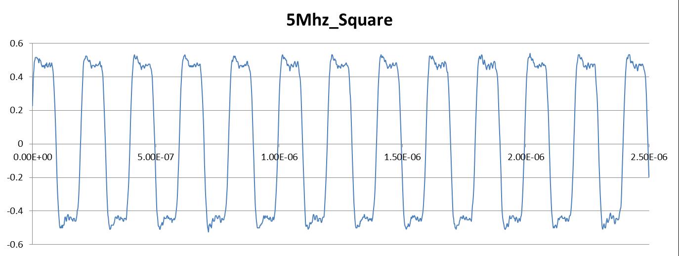
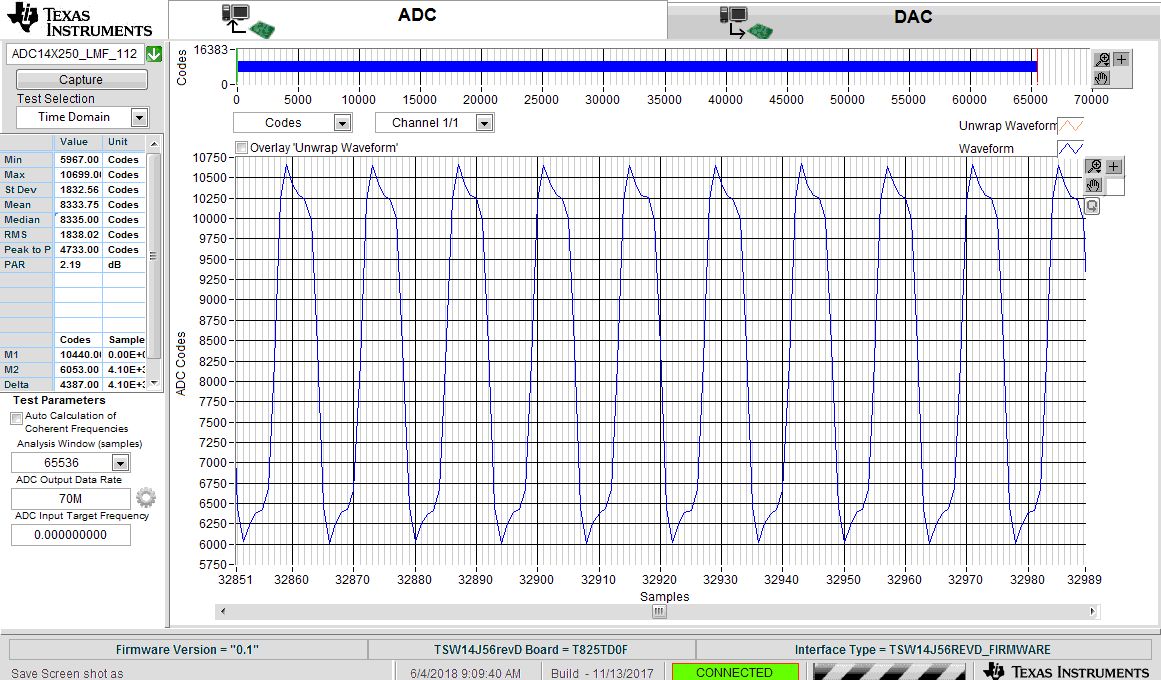
I am using the clock frequency of 70Mhz, and my maximum signal frequency is 5Mhz.

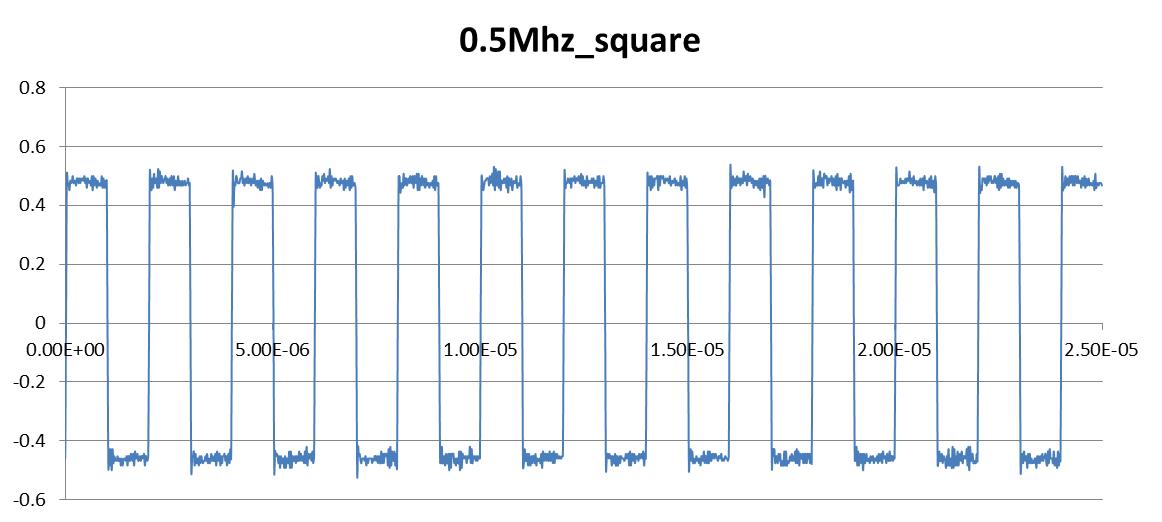
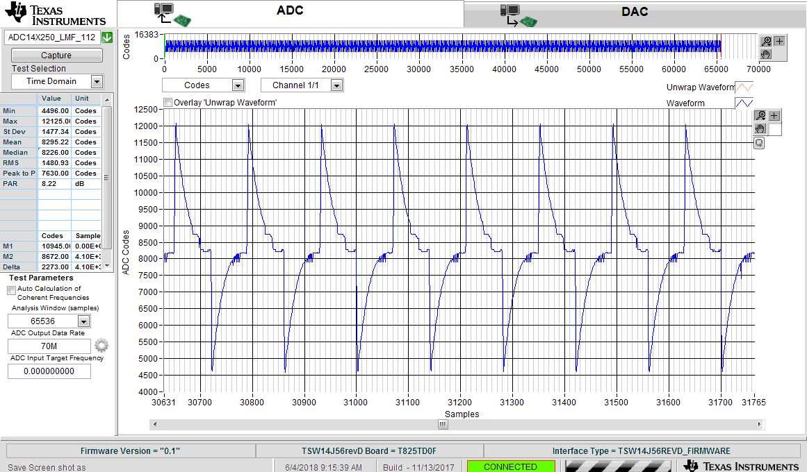
At 5Mhz, I was able to capture the waveforms from the signal generator with some errors, then I started reducing the frequency of the signal with hopes of getting better resolution and less distortions, but I realize that as I decrease the frequency, my signals get more distorted. Why is this happening and how do I fix this?

Below I have included the figures of waveforms from oscilloscope (input signal waveform) and HSDC pro capture for frequencies of 5Mhz and 0.5Mhz. The clock frequency for both the cases is 70Mhz and provided by TSW2170EVM.

  • Hi Lizon,

    We are looking at your question and we will get back to you soon.

    Regards,
    Neeraj
  • Hi Lizon

    The ADC14X250EVM input signal path uses back to back baluns to convert the 50 single ended input to a differential format compatible with the ADC inputs.

    The baluns used have a lower frequency limit of 5 MHz. https://www.macom.com/products/product-detail/MABA-007159-000000

    C20 and C21 will also contribute a high-pass effect to the signal path.

    Therefore signals below 5 MHz will not be properly passed by the transformers, so you'll get the high-pass response that you are seeing.

    If you want to convert signals that are lower frequency, or DC you will need to modify the board to utilize the resistor coupled differential path from VIN+/VIN- input connectors to the ADC inputs. To get good performance this signal must be driven differentially, and the common mode must match the VCM voltage output by the ADC. If you signal source is not already differential you may need to use a DC-coupled differential amplifier EVM to convert your single ended signal to a compatible differential output.

    I hope this is helpful.

    Best regards,

    Jim B

  • Hi Jim,

    That did help but I have some follow up questions. According to what you have said, I am planning modification of the board.
    Following will be my steps, could please take a look at it and see if I have this right:
    1. Remove R15 and populate R4
    2. Remove R1, R52, R2, R53, and populate R12, R13, R5, R6
    3. Measure VCM (TP15) voltage, make sure the common mode voltage has the same voltage as VCM.
    4. The input signal should have common mode voltage of VCM, and differential signal on top without exceeding the max rating of +/- 0.75V.

    The only question I have: The VCM value that ADC outputs is a constant value correct? It would not fluctuate in the middle of operation, and it does not depend on the input signals?
  • Hi Lizon

    Your list is close, but is missing the removal of R3.

    1. Remove R15, R1, R2, R3, R10, R52, R53.
    2. Install R5, R6, R12, R13. 
    3. Apply differential input signal to J2 and J3.
    4. Signal must be balanced such that (VIN+ + VIN- / 2) = VCM+/- 50mV.

    It may be possible to externally adjust the amplifier VCM to meet the requirement listed above, but the general approach is to connect the ADC VCM output voltage to the amplifier VCM control input. This way if the ADC VCM does change over temperature, etc. the amplifier will automatically track.

    As you note, it is also important to ensure the amplifier outputs do not exceed the capabilities of the ADC inputs which is VCM +/- 0.75V. This may require using an amplifier with an active clamp, or adding clamping components at the amplifier outputs. The amplifier should only be enabled after the ADC has been powered up and the VCM voltage has stabilized.

    An alternative to this approach would be to select a different ADC EVM that already incorporates an amplifier drive stage and can therefore support lower frequency or even DC coupled inputs. The TSW54J60EVM is one such EVM.

    I hope this is helpful.

    Best regards,

    Jim B

  • Thank you Jim.
    I will try this next.
    Lizon