This thread has been locked.

If you have a related question, please click the "Ask a related question" button in the top right corner. The newly created question will be automatically linked to this question.

[FAQ] PCB Layout Guidelines and Grounding Recommendations for High-Resolution ADCs

Other Parts Discussed in Thread: LM27762

I am laying out a PCB that uses a precision 24-bit ADC. What are TI's recommendations for PCB layout?

Also, should I split the ground plane between analog and digital circuits?

  • For any product specific layout guidelines, please refer to the the datasheet:

    Our datasheets usually contain a Layout Guidelines section...


    as well as a Layout Example...


    For general PCB layout guidelines please refer to the following resources:


    PCB Grounding

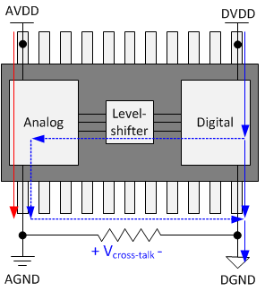
    There are two common approaches to PCB grounding when working with mixed signal devices:

    1. Separate (split) analog and digital ground planes
      Analog circuitry is typically very sensitive to noise so to prevent digital switching noise from coupling into sensitive analog circuit nodes, separate grounds planes are maintained so that digital return currents do not flow on the analog ground plane. Even though grounds are separated, they must usually be connected together at some point to allow analog, digital, or mixed signal devices to communicate with each other.

    2. Single ground plane for both analog and digital circuits
      Alternatively, analog and digital circuits can be partitioned into different regions or areas on the PCB. Digital return currents are kept separate from the  sensitive analog circuitry by controlling the distance between these circuits (See http://www.ti.com/lit/wp/snaa113/snaa113.pdf for details regarding the path of return currents). By providing one large ground plane, the ground plane impedance is reduced and so is the common-impedance coupling between signals.


    While there is no one right way of laying out a PCB, we see some advantages to using the 2nd method (the single-ground plane):

    • From an EMI perspective, a single solid ground plane is less likely to radiate or receive RF signals.
      Notice that the shape of a split-ground plane looks similar to that of a dipole antenna:

      It is not only the shape of the ground plane which impacts the potential EMI performance but many other factors as well. For some additional information on PCB layout and it's effects on EMI performance, I highly recommend this excellent three part article series on EDN:

      [EDN] Design PCBs for EMI, part 1: How signals move

      [EDN] Design PCBs for EMI, part 2: Basic stack-up

      [EDN] Design PCBs for EMI, part 3: Partitioning and routing


    • The split-ground plane layout approach is more prone to current loops when traces are routed poorly.
      Both layout approaches depend on partitioning analog and digital circuits on the PCB. However, if the partitioning is not implemented correctly or if traces need to cross over the ground plane split or gap in the split-ground layout then a large loop area is created. This loop makes the trace impedance much more inductive and can result in signal integrity issues, such as ringing. Additionally, if multiple return currents are forced to flow through a small ground plane connection, they will be prone to common-impedance cross-talk.

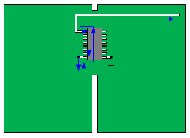
      Poor trace routing can lead to large current loops (poor signal integrity) and cross-talk through common-impedance coupling Bridging the trace above the ground plane connection and widening the ground-plane connection results in better signal integrity and less signal cross-talk

      NOTICE: The split-ground plane implementation in the right image is starting to approach that of a single ground plane layout!


    • Analog and digital grounds on most ADCs are not isolated and they require a low-impedance connection between them!

      If you are going to split the analog and digital ground planes, then you MUST MUST MUST connect the analog and digital grounds together at the ADC, not elsewhere on the PCB (see the right image above)! There are a couple of reasons for this:

      1. Voltage differentials of 0.3V or more between the analog and digital ground may damage the ADC (see the Absolute Maximum Ratings table in the datasheet). In cases where there is an AVSS pin (bipolar supply option) instead of AGND (unipolar supply only), then AVSS may go lower, see below...


        In the split-ground plane approach where these grounds are not connected together near the ADC, this connection will be inductive. Inductive traces are prone to voltage spikes during current transients, so keep the impedance between grounds as low as possible to avoid damaging the ADC!

        NOTE: If you're using a bipolar analog supply (e.g. AVDD = 2.5V and AVSS = -2.5V), the "analog" ground is still at 0V. When analyzing analog return current paths, make sure there is a low-impedance path back to the "ground reference" of the components that are generating the +/- 2.5V supplies. For example, if you use the LM27762 as your supply source, then consider the "GND" pin of the LM27762 to be the analog ground, to which all analog return currents will flow back to.
          
         
      2. Internal to all non-isolated ADC's is a level-shifter that goes between analog and digital circuit functions. Without this level-shifter, the digital controls would not be able to operate any of the ADC's analog functions. For this level-shifter to work properly, the analog and digital grounds of the ADC must be at (or nearly at) the same potential.


        NOTE: For any internal signals that are routed through this level-shifter, their return currents will need to flow back to their source. Therefore, there will be some digital currents flowing on the analog ground plane! To prevent these currents from having an effect on the AGND voltage and coupling into sensitive analog circuitry, it is best to keep the connection between analog and digital grounds as short (low-impedance) as possible to minimize "Vcross-talk".