This thread has been locked.
If you have a related question, please click the "Ask a related question" button in the top right corner. The newly created question will be automatically linked to this question.
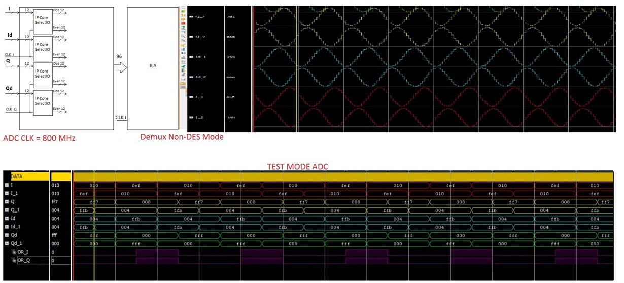
The ADC receives a clock frequency of 800 MHz. ADC Demux Non-DES Mode.
CAL_ADC = 0
DDRPH_ADC = 0
ECE_ADC = 0
CALDLY_ADC = 0
FSR_ADC = 0
NDM_ADC = 0
TPM_ADC = 0
PDI_ADC = 0
PDQ_ADC = 0
DES_ADC = 0
Configuration register 0x2010. CLK_I and CLK_Q 200 MHz. Data is sent to SelectIO. I connected to the output of SelectIO ILA. I get odd data inverted. ADC test mode data is correct.
Hello Jim! Jim, thanks! You helped me well. I understood what was going on. The input SelectIO data bus is limited. The bus can not be more than 16 bits. It is necessary to use 4 SelectIO components in channels I, Id, Q, Qd. I wanted to use the differential frequency CLK _I and CLK _Q. Vivado does not allow to connect differential conductors to several components. I connected the differential wire CLK _I_diff and CLK_Q_diff using BUFDS. I received a non-differential CLK_I and CLK_Q. CLK_I is connected to SelectIO_I and SelectIO_Id. CLK_Q is connected to SelectIO_Q and SelectIO_Qd. I do not need to use SelectIO? I need your help on how to properly process data from the ADC. Do you have sample code?
Hi Nikola
Please see the FPGA firmware source contained in the ADC12D1600RB/ADC12D1800RB Design Package which is available in the software section of this web page:
http://www.ti.com/tool/adc12d1600rb
I believe in this firmware only one of the DCLK inputs is used to clock all 4 banks of data into the FPGA.
I hope this is helpful.
Best regards,
Jim B
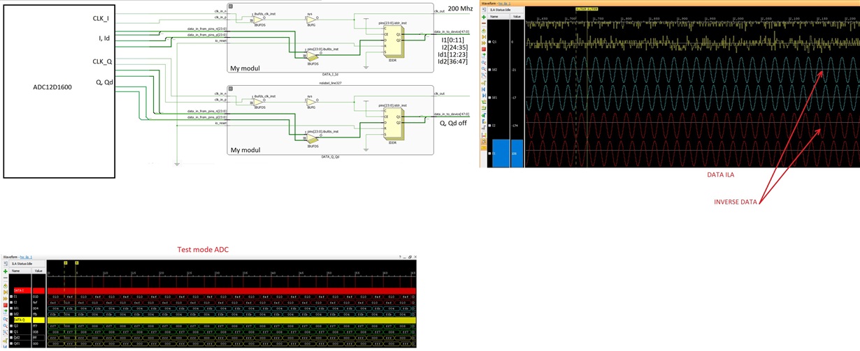
Hello Friend! I changed my project. I created a component with 24 differential inputs and 48 output data buses. Data from channels I and Id are fed to the input. Differential clock CLK_I is connected to the input for data I and Id. Differential clock CLK_Q is connected to the input for data Q and Qd. I turned off the channel Q. Data is transmitted only on the I and I channel. Replacing the IP core of the SelectIO did not change the result. The data channel is inverse between measurements. I turned on the ADC test mode to check the channels. The test is normal. What is the problem? If the FPGA does not work correctly, why does the test pass normally?
I looked at the data from the ADC. I sent the channel I data to ILA. To view the data that is negedge clk_I, I recorded the data in a 12-bit register clocked negedge clk_I. I sent the recorded data to ILA. The result is the same. Even and odd data are inverse.
Hi Jim! I studied your examples. I accept the data from the ADC as in your example. Your example uses BUFDS and IDDR. I do that too. I in the message above loaded the scheme of the project. I tried a different design. I tried IP core XILINX. I tried my modules. I tried to look at the data from BUFDS. I always got the same result. The problem is not in FPGA. How do I check the ADC? Mode other than TEST MODE? This mode will not show fully the operation of the ADC. In this mode, the ADC sends a number and an investment number.
Hi Jim! Sorry for not immediately answering, I was busy. I put aside this board with ADC12D1600 ADC. I have a board with ADC ADC08D1500 and FPGA. I decided to check correctly I accept the data from the ADC. This ADC is similar to the ADC12D1600, it is only 8 bit, the speed is lower and the control is slightly different. I checked my design. I received the correct data in DDR mode. Now I’m sure that I’m doing everything right. I checked the connection of the ADC and PCB.
My ADC12D1600 Sampling Clock CLK = 800MHz data clk DCLK = 200 MHz. I connected DCLK to the pin FPGA DCLK = 200MHz and measured the frequency on the pin. I will try to lower the Sampling Clock. At 50 Mhz, should I set bit 8 in the Configuration Register?
Hi Jim! I solved the problem. The synthesizer did not set the necessary frequency. Incorrect frequency posumala on demodulator. Since the demodulator is not the correct data received on the ADC. Thanks for the help. Now everything is working fine.