This thread has been locked.

If you have a related question, please click the "Ask a related question" button in the top right corner. The newly created question will be automatically linked to this question.

ADS8867: Analog ADS8867 16bit SPI IC issue

Part Number: ADS8867
Other Parts Discussed in Thread: OPA313, INA333, INA133

Hello,

I have handed over design that uses ADS8867 for Wheaton Bridge reading. O/P of that bridge is 80mV and gain before feed to ADS8867 is 11x.

AINN is 1.25V, AINP is output from OPAMP and Vref is 2.5V.

The reading I would expect is at 0 pressure around AINN(offset), right? Also at full output I am getting hex reading of 0x26c2.

Can some one please help me understand that this reading (DAta) is after OFFSET removed? or please direct me to some appropriate APP note.

Thanks

Jigar

  • Hello Jigar,

    Can you provide a schematic that includes the bridge, amplifier, and ADS8867?

    The conversion reading is in 2's compliment. A conversion code of 0x26c2 indicates an input differential voltage of about 757mV when using a 2.5V reference. If AINN is fixed at 1.25V with respect to ground, then AINP should measure around 2.007V.

    Take a look at this circuit for measuring a bridge.

    www.ti.com/.../sbaa245a.pdf

    Regards,
    Keith N.
    Precision ADC Applications
  • Can you please explain me your calculation to get 757mV?

    Thanks
    Jigar
  • Hello,

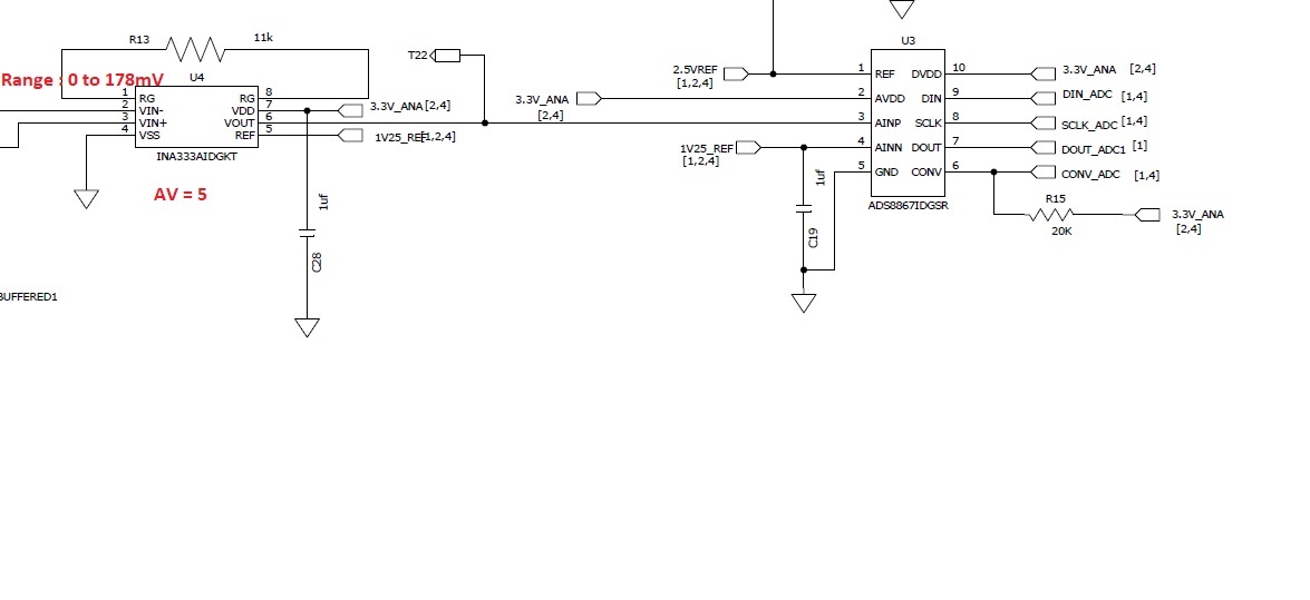
    Based on my circuit and gain i will not have more than 1.25V on my AINP.

    Please look at attached circuit and let me know if anything not make sense.

  • Hello Jigar,

    If you are driving the input of the ADS8867 directly with the INA333, you will need an RC filter and you will be limited to around 10ksps max sample rate to get rated performance. If you want to achieve 100ksps, then I suggest adding an OPA313 buffer with an RC filter similar to Figure 61 in the datasheet.

    Regarding the input calculations, since AINP<1.25V max and AINN=1.25V, AINP will always be less than AINN, and the ADS8867 will convert this as a negative differential input result. Figure 44 in the data sheet shows the transfer characteristics. With AINP=0V, the ADC will see a differential input voltage of -1.25V, and the conversion result will be 0xC000. With AINP=1.25V-1LSB, where 1LSB=76.3uV, the conversion result will be 0xFFFF.

    A conversion result of 0x26c2 is the decimal equivalent of +9922. The differential voltage on the inputs of the ADC would then be equal to 9922*1LSB=9922*76.3uV=0.756988V, or rounded to 757mV.

    Regards,
    Keith
  • Thanks Keith,
    In the case of 0x26C2 where O/P is calulated 757mV, We still can do 1.25+.757 = 2.0 V as AINP?my gain is 11 not 5 so AINP will be 0.182 Which make sense. But when I calculate for 000e which is almost 0V it gives me AINP 0.111 which is not correct. Can you please let me know. Range should be 0 to 182mV of sensor....
  • Hi Jigar,

    Based upon your schematic above, you have a gain of 10.1 (11k resistor on Rg pins of INA333) and Vref=1.25V for INA133. The output of the INA333 (connected to AINP) with 0V differential input will be 10.1*Vin-diff+1.25V, or 1.25V. With Vin-diff=178mV, the output of the INA333 will be 10.1*0.178V+1.25V=3.046V. At this point, you will be exceeding the ABS MAX input voltage rating of the ADS8667. The INA333 will current limit to around 40mA, but this could be enough to cause the ADC to latch-up and cause permanent damage. Adding a 1kohm resistor between the INA333 output and the ADC AINP pin will limit this current to a safe level, but you will still not be able to get correct readings in this condition.

    The maximum input voltage on AINP is limited to Vref+0.3V. Using a Vref=2.5V, the maximum input voltage will be limited to 2.8V. This will set a maximum input differential voltage on the INA333.

    2.8V-1.25V/10.1=153mV.

    For an input differential voltage at the INA333 inputs, Vin-diff = (VIN+ - VIN-), you should get the following:

    Vin-diff=0V, AINP=10.1*Vin-diff+1.25V=1.25V. With VINN=1.25V, the ADS8867 should give a conversion result of (AINP-AINN)/Vref*2^15 = 0x0000h.

    Vin-diff=153mV, AINP=10.1*0.153V+1.25V=2.795V. With VINN=1.25V, the ADS8867 should give a conversion result of (AINP-AINN)/Vref*2^15, (2.795-1.25)/2.5*2^15=20254d=0x4F1Eh.

    In order to measure input differential voltages at the INA333 inputs up to 178mV with a gain of 10.1, you should decrease the 1V25_REF voltage. Setting this voltage to 0.5V will allow measurement of the input differential voltage from 0->178mV.

    Regards,
    Keith
  • This resolved and confirmed my design.

    Thanks Keith.

    Thanks

    Jigar