This thread has been locked.

If you have a related question, please click the "Ask a related question" button in the top right corner. The newly created question will be automatically linked to this question.

ADS114S08B: EMC Robustness Documentation

Part Number: ADS114S08B
Other Parts Discussed in Thread: TVS1401

Hello All,

My customer is developing an application that will acquire up to 6 input thermo resistances and output some over-temperature levels.

My customer and I are wondering whether there are any reference designs or applications in which there are some suggestions to increase the EMC robustness that is the most critical requirement for customer application.

Many Thanks,

Antonio

  • Hi Antonio,

    Unfortunately we don't have a specific design example.  This is a rather complicated topic in which books have been written.  I often refer to the book Electromagnetic Compatibility Engineering by Henry Ott.  There are many pieces to the puzzle, and PCB layout plays a very large role.

    The method(s) of protection used will greatly depend on what types of interference you are trying to protect against.

    1. EFT
    2. ESD
    3. EMI
    4. RFI
    5. Power line-cycle

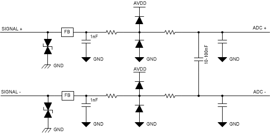
    Each of these types have similarities as well as differences.  Depending on levels, frequency and duration, not one single method of treatment will prevent all noise sources from affecting the system.  Below is an example of various treatment and stages in the input path.

    Anything that is placed in the input path can cause error in the measurement unless extreme care is taken to choose the proper components.  Diodes must be low leakage (nA) as opposed to leakage in uA.  The first and primary goal is to protect the ADC from an overvoltage/overcurrent condition where the device absolute maximum ratings are exceeded.  In general the maximum input voltage would be +/-300mV from the analog supply rail, with a maximum input current of 10mA.

    Following the diagram from left to right, there is first a bidirectional TVS diode connected to earth ground.  This diode will protect the system from high power transients.  TI makes a flat-clamp TVS diode, such as the TVS1401, that clamps the response to a flat voltage level compared to traditional TVS diodes.

    Following the TVS diode is a ferrite bead (or bead combination) that creates a low pass filter with the adjacent capacitor when high frequency content enters the system from EMI/RFI.

    Following the first filter is a resistor and diode stack.  The diode stack should also be low leakage, such as a BAV199, or BAV199W.  This diode will prevent the residual overvoltage from the TVS diode and prevents high currents or transients from entering the ADC.  The series resistor will limit the current through the diodes. 

    The last stage is the traditional RC low pass filter for Delta-Sigma ADCs.  Usually the differential cap ranges from 10 to 100nF.  The common-mode caps should be at least 1/10th or smaller than the differential cap to limit drift affects of filter mismatch.

    Not all of the components are required.  What is actually used will depend on what types of noise are expected to be seen within the system, as well as available space to place the components.

    Best regards,

    Bob B