This thread has been locked.

If you have a related question, please click the "Ask a related question" button in the top right corner. The newly created question will be automatically linked to this question.

DAC37J82EVM: Synchronization time varies by 1 LMFC period

Part Number: DAC37J82EVM
Other Parts Discussed in Thread: DAC38J84
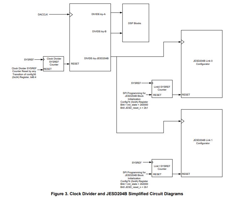
Setup Details :

  • DAC37J82EVM board
  • Xilinx VCU118 Demo board
    • JESD204 v7.2.4 TX IP is instantiated
  • JESD204B subclass 1
  • LMFKS = 4, 2, 1, 30, 1
  • 1 GSPS sampling rate, 250 MHz core clock, 10 Gbps line rate

Observations :
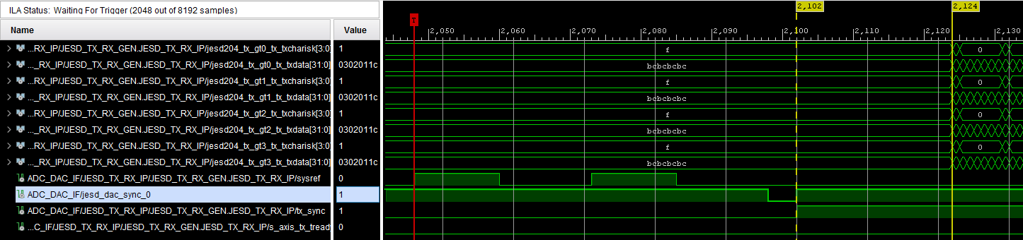
On most synchronization attempts, the DAC requests SYNC from the FPGA 130 ns after the rising edge of SYSREF is seen :

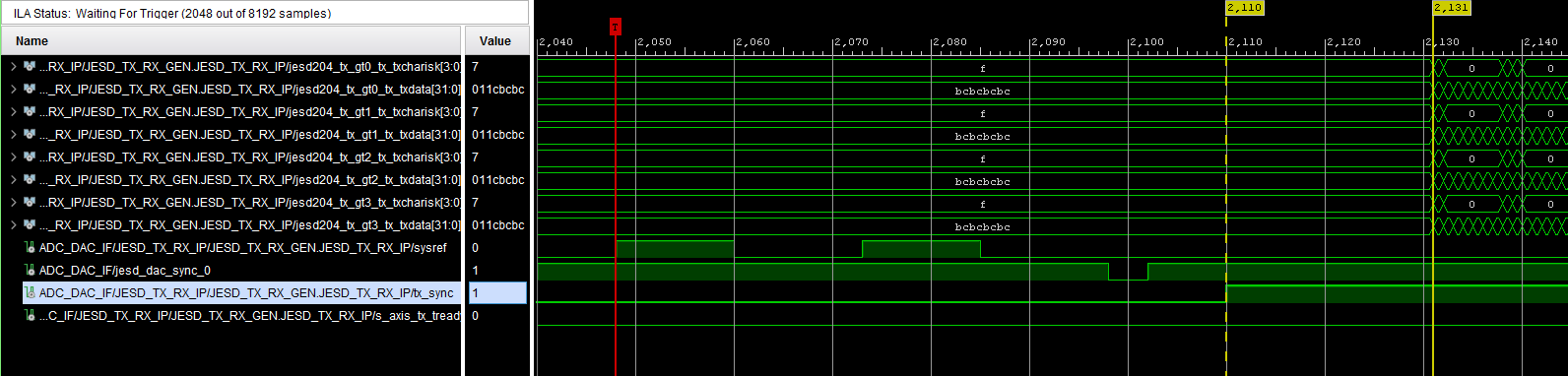
However on a minority of synchronization attempts (5% - 10% of tries), the DAC requests SYNC from the FPGA 100 ns after the rising edge of SYSREF is seen :

I've verified on a high-speed scope that the DAC is given 2 ns of setup time to capture SYSREF, so I don't believe that's the issue.

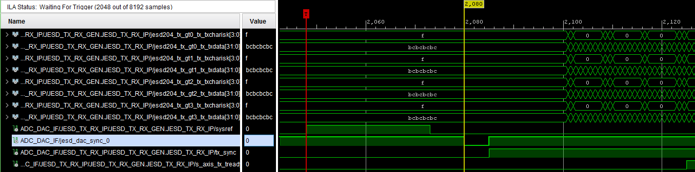
This leaves us with a variance in synchronization time of 1 LMFC period (30 ns in our case), and I'm struggling to understand why this would be. Based on what I have learned about the JESD204B protocol so far, I thought that the rising edge of SYSREF was supposed to realign the LMFC in all connected devices and that ILA generation begins on the next LMFC zero crossing after SYNC has been deasserted, as indicated in this image :

How does the DAC decide on which LMFC edge to request SYNC from the FPGA? Is there a way to force the DAC to use the same LMFC edge for SYNC requests every time?


Thank you

-Branden

  • Hi Branden,

    We can refer to the following app note for some debug

    http://www.ti.com/lit/an/slaa696/slaa696.pdf

    There are two main blocks within the DAC38J84 family: the clock divider for the whole logics, and also the JESD204B RX IP.

    It is possible that we may need to delay the sequence of the clock divider and JESD204B RX IP synchronization with respect to your overall system timing. In your case with only 1 pulse sysref, we may need to increase to total of two pulses, with the first pulse setting up the overall clock divider, and the second pulse coming in to synchronization the JESD204B RX IP

    We will also need to review the SPI register writes to these key critical synchronization circuits with respect to the SYSREF trigger. We will need to write to these registers first to first "arm" the logic, while triggering the SYSREF pulse to fire the synchronization logic.

    lastly, you will need to check to make sure the single pulse SYSREF, if in AC coupled situation between the SYSREF driver and DAC38J84 sysref receiver, need to have good starting common mode for the SYSREF to properly settle within one pulse. a few customers of ours seen these type of SYSREF variation due to the common mode needing to be charged up between the caps. If necessary, you may start the SYSREF in continuous mode way before the whole initialization sequence to ensure good common mode establishment.

  • Hi Kang,

    Thank you for the response, there is a ton of information that I found very helpful in that app note. I tried following your advice, but I am seeing the same issue unfortunately.

    I perform the following register writes between synchronization attempts :

    0x4a --> 0x0f3e //assert jesd_reset_n
    0x24 --> 0x0020 //arm the main clock dividers to reset only on the next SYSREF pulse
    0x5c --> 0x3333 //arm the JESD clock dividers to skip one SYSREF pulse and then reset only on the following one
    0x4a --> 0x0f3f //deassert jesd_reset_n
    0x4a --> 0x0f21 //set init_state to 0b0000

    Based on how I understand the architecture, I thought it would be reasonable to try resetting the main clock divider with one SYSREF pulse, and then writing 0x0000 to register 0x24 and 0x1111 to register 0x5c so that the main clock divider is never reset again and the JESD clock divider responds to every SYSREF pulse. My sequence of register writes in this case was :

    0x4a --> 0x0f3e //assert jesd_reset_n
    0x4a --> 0x0f3f //deassert jesd_reset_n
    0x4a --> 0x0f21 //set init_state to 0b0000

    This didn't seem to produce any different results though.

    Also thanks for the reminder about AC coupling SYSREF. We are using the default SYSREF connection on the EVM from the LMK which is DC coupled, so I think we're fine there.

    Are there any other obvious steps to take at this point? I will reply with any new developments that I come across on my end.

  • Hello Branden,

    Regarding

    Branden Buckner said:
    0x4a --> 0x0f3e //assert jesd_reset_n
    0x24 --> 0x0020 //arm the main clock dividers to reset only on the next SYSREF pulse
    0x5c --> 0x3333 //arm the JESD clock dividers to skip one SYSREF pulse and then reset only on the following one
    0x4a --> 0x0f3f //deassert jesd_reset_n
    0x4a --> 0x0f21 //set init_state to 0b0000

    I recommend doing the following

    1. make sure the FPGA JESD204B TX IP is properly reset and ready to register the SYNC~ from the DAC38J84. The JESD204B standard requires the JESD204B TX (FPGA) side to be ready before the JESD204B RX (DAC) side. This is to ensure that the JESD204B TX can see and register the ~SYNC signal in time and transmit K28.5 when ready.

    2. set SYSREF to idle

    3. execute the following code

    0x4a --> 0x0f3e

    0x24 --> 0x0000  //reset the main clock divider sysref counter

    0x24 --> 0x0020 //arm the main clock divider sysref counter

    0x5c --> 0x0000 //reset the JESD204B RX IP sysref counter

    0x5c --> 0x3333 //use the 2nd sysref pulse

    0x4a --> 0x0f3f //deassert JESD_reset_n 

    0x4a --> 0x0f21

    4. trigger the SYSREF from the clocking chip. Measure the time of the trigger of the SYSREF clocking chip with respect to the ~SYNC pulse.

    Regarding the timing of the ~SYNC pulse, I have two thoughts:

    1. I saw that your SYSREF is now periodic in this picture (or at least gapped periodic). Please double check if there are any potential asynchronous behavior of the trigger to the SYSREF in the clock chip with respect to the ~SYNC pulse (which should be deterministic). I suspect that if the clocking chip SYSREF is triggered in asynchronous behavior (i.e SPI bus), then the uncertain in ~SYNC response time would be in essence the variation of the asynchronous behavior

    2. If you can ensure the SYSREF starts at the same relative phase from start-up to start-up, then the timing of the ~SYNC pulse will *not* impact deterministic latency. Basically, the latency through the DAC38j84 is determined by the SYSREF alignment of the LMFC. Yes, you will see a absolute time difference of LMFC cycle, but the relative latency (from entrance to ext of the DAC38J84) will be the same. Basically, the data goes through FIR filters, inteprolation stages in the same latency. 

    The only thing absolute is the starting phase of the TXNCO, which could be time stamped in absolute term of SYSREF trigger edge or the starting of the first LMFC synchronization. In this case, I recommend that you resync the TXNCO again with SYSREF to ensure the timing of the starting phase of the NCO are reset at the same absolute time.

    I mention this because there will be cases where the JESD204B RX IP of the DAC will pull sync low due to various errors such as 8b/10b coding error or other errors. The JESD204B will do its best in its own environment to go through re-handshake and complete resync again. If your system is based on absolute timing fo the ~SYNC event, then I believe you will have some difficulties in some scenarios where re-handshakes is a must. 

  • Hi Kang,

    I tried modifying my sequence of commands before attempting synchronization like you suggested, adding in commands to reset the clock dividers before arming them. I didn't notice any difference in behavior though.

    I am indeed using a gapped periodic SYSREF with 2 pulses. The pulses are generated from the clock conditioner device and triggered by the VCU118 through J22 on the EVM and the SYNC/SYSREF_REQ pin on the device. the logic on the VCU118 responsible for requesting SYNC is clocked from one of the outputs of the clock conditioner itself, so that whole interface is controlled synchronously.

    You're right that the way our system is designed, we rely on SYNC to be deasserted at a predictable and consistent time between power cycles (ultimately driven by the precise time at which we're able to start transmitting and receiving RF information) so rehandshakes will be a challenge for us to handle. In the worst case we may be forced to resynchronize the entire system if we experience an error on one of the links.

    I did come up with a solution that I think will work for us, but it's not one that I'd call ideal. The idea is that the DAC always deasserts SYNC on and LMFC edge, we just can't guarantee which one. To account for that, I've added logic in the FPGA to hold its SYNC input low until the latest LMFC edge that the DAC would deassert SYNC. At that point, the FPGA SYNC input is allowed to follow what it's getting from DAC. In the images below, jesd_dac_sync_0 is the raw sync signal output by the DAC, and tx_sync is the signal that the FPGA passes to its JESD IP. I think this solution is valid in this case since SYNC is not a timing critical signal in JESD204B subclass 1. As long as it's deasserted after an LMFC edge, the JESD TX IP in the FPGA will start transmitting its ILA sequence on a subsequent LMFC edge. Like I said this is not ideal in the general case, but it keeps us moving forward. If I find a combination of DAC register settings or discover a flaw in my test setup I'll make sure to post an update here to make everyone aware of a better solution.

    Thank you for all your help,

    -Branden