This thread has been locked.

If you have a related question, please click the "Ask a related question" button in the top right corner. The newly created question will be automatically linked to this question.

ADS1258: ADS 1258

Part Number: ADS1258

Hi,

I am unable to get the accurate readings for the ADS 1258 interfaced to ST micdlawsas1-01-mk2-0a-sd.pdfro controller in our design. I had referred to other posts in the forum regarding the design and identical problems.

Following are the deviations observed in our design with reference to other posts:

  1. Add 47 ohms termination resistors for ADC serial interface.
  2. Add a low pass RC filter of 150 Hz at output stage of OpAmp or external signal conditioning circuit of ADC.
  3. Add a buffer to reference voltage generator and a differential filter capacitor between VREFP and VREFN to help stabilize and reduce the voltage reference noise.
  4. Following is the ADC layout.

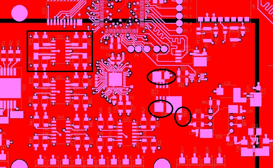
Deviations observed in analog and digital grounds and placement of the Rg and Rf in the op amp stage are highlighted in the above picture.

Please do suggest me any changes required apart from the above mentioned points to correct the problem with accuracy.

Schematics and readings observed are provided in the attachment.ADCReadings.xlsx

  • Hi Kongara,

    Welcome to the E2E forum!  Thanks for providing the schematic, layout and data.  Regarding the data, where are you applying the voltage and where are you measuring the voltage?  You have a significant path that include TVS diodes, shunt resistances on some inputs, and an op amp in a gain of 2 configuration.  I would suggest attempting to limit the source of the error to see if it is the ADC where there error occurs or through the system path.  To determine the true error of the ADS1258 you should measure at the ADC inputs and not at the system input.

    For the actual data I would like to see unconverted results.  In other words the raw output code in hex that you are getting from the ADS1258.  For the op amp you are using there is a typical offset of 3mV.  This seems to correlate with your data near 0V.  The rest of the error appears to be gain error.  Here again it would be good to understand the source of the gain error.  If the error is from the op amp, then you should see a significant difference from the input of the op amp to the output.  Another thing you could try as an experiment is to make the op amp a straight buffer without gain.

    The items you mention that differ from other posts and your schematic primarily relate to noise.  Many of these recommendations are in the ADS1258 datasheet.  For example there is a section on Aliasing (page 20) and using series resistors on the digital lines (Hardware Considerations section 'g' on page 42). 

    In review your schematic I did notice a few things.  My biggest concern is with the analog and digital grounds.  For best performance when using a unipolar analog supply is to tie the AVSS and DGND pins together with a low impedance connection as close to the ADS1258 as possible.  For this type of operation AVSS and DGND should not separate by more than 300mV.  If they do, then the Absolute Maximum Ratings can be exceeded and damage to the device may occur.  Adding an inductive path or even a ferrite in certain conditions can drive AVSS and DGND apart significantly.  Also, schematically some of your analog bypass caps connect to the digital ground at the ADS1258.  For example C13, C14 and C94. Also the crystal capacitors are connected to digital ground instead of analog.  So these connections follow an inductive path and are not optimal.

    I also noticed that with some of the LDOs used the input cap is tantalum with a working voltage less than the 12V battery supply voltage.  One such case is C89 at the input to U21 that supplies the analog voltage to the ADS1258.

    As you are replicating the input op amps many times over, have you considered using a single input combination using the MUXOUT and ADCIN connections on the ADS1258?  This could reduce the multiple op amps you are using to a single op amp.

    You might also consider looking at different TVS diodes with lower leakage.  The one you are currently showing has leakage at 1uA.

    Best regards,

    Bob B

  • Hi Bob Benjamin,

    As suggested, i had provided reading at Op amp input , out put and ADC input along with ADC out put Raw values in the attachment.

    Following values are read from ADC registers 

    Gain Raw: 0077E0D5    0.998985
    Vref Raw: 003BCFF9   4.984366

    Following are the equations used to convert the ADC raw value to Voltage equivalent

    Gain = ChannelValue  / 7864320

    Vref = ChannelValue   / 786432

    ChannelValue  = ChannelValue * Vref

    ChannelValue  = ChannelValue / 8388607.0F

    ChannelValue = ChannelValue/ Gain

    OpAmpStageValues.xlsx

  • Hi Kongara,

    Thanks for the data as that tells us a number of things, but unfortunately doesn't answer everything.  First of all I would like to point out that the full-scale range of the ADS1258 is not +/-Vref, but rather +/- 1.06(repeating) * Vref.  This is discussed on page 25 of the ADS1258 datasheet.  So what this means is all of your calculations are a bit off and should be higher than what you show in the spreadsheet.

    Second thing is the op amp cannot drive close to ground.  This is clearly shown by the first few readings and the first input voltage that is tracking at all with the input is the 50mV input case.  

    I've attached my updates to your spreadsheet data by adding 3 new columns.  The first added columns uses the correct value of LSB using a 5V reference with the calculation shown in Volts.  The second column shows the difference of the ADC output relative to the measured value of the output op amp.  These numbers should match.  If you compare strictly to the op amp input, then you will include not only the offset of the op amp but any gain error as well.  To really evaluate the precision of the ADS1258 you need to measure the input and then compare to the ADC result.  To reinforce what I just mentioned the third column shows the difference of the ADC result to the input.

    If we look at the voltage follower case and the center column, notice that up to 50mV the difference is large.  Again this is due to the op amps inability to drive close the ground.  After 50mV the input/output is pretty consistent.  This most likely is the true offset of the op amp.

    With voltages greater than 1V input, it is difficult to explain what is being shown.  This appears to be gain error, but it is much greater than what I would expect from the ADS1258.  You can correct for the ADC offset and gain error by following the information in the datasheet on page 26 pertaining to Internal System Readings.  Keep in mind that this only corrects error as it relates specifically to the ADS1258 and will not fix gain error from the op amp.

    OpAmpStageValuesBob.xlsx

    Best regards,

    Bob B