This thread has been locked.

If you have a related question, please click the "Ask a related question" button in the top right corner. The newly created question will be automatically linked to this question.

TLV2545 optimal layout

Other Parts Discussed in Thread: TLV2545

Hi There,

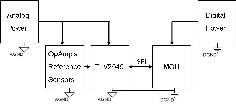
I am in process of laying out a 4 layer board that contains a tlv2545 12 bit ADC.  I have seperated digital and analog grounds and power that are tied together in one location.  It is not clear to me how this device is intended to be laid out.  

I took a look at the user manual for this device and it shows the EVM board that contains a variant of this ADC.  It appears that the EVM board has the TLV254x grounded to the analog plane and powered from the digital plane?  There is no mention of best alyout in the datasheet.

Can you recommend best layout for this chip based on it's internal architecture?  

Would you recommend the seperate analog and digital power and ground as on the EVM board?  Or use the analog plane with the digital lines being fed at the edge of the digital plane?  Or other?

Thanks


  • Hello MJ,

    This EVM was designed in 2003, and we currently try to avoid the use of split ground planes. For a while now, we have been designing EVMs that meet datasheets specs using a single ground plane even for converters with higher resolution and speed than the TLV2545.  

    The most critical aspect in the layout is to keep the analog signals paths (VREF, Vin+, and Vin-) away from the digital signal paths (CS, SCLK, and SDO) .

    The converter should use analog power. The power for the Vdd pin should come directly or regulated down form the analog power. For this same reason, the GND pin should be connected to analog ground.

    I hope the following diagram clarifies the way powers and grounds should be treated.

    Regards,