This thread has been locked.

If you have a related question, please click the "Ask a related question" button in the top right corner. The newly created question will be automatically linked to this question.

DAC37J82EVM: Need proper config settings for LMK04828 and DAC37J82

Part Number: DAC37J82EVM
Other Parts Discussed in Thread: DAC37J82, LMK04828, DAC37J84, DAC37J84EVM

Hi,

I'm using the DAC37J82EVM alongside an FPGA board.

The clocking is set up as captured in the screenshot below.

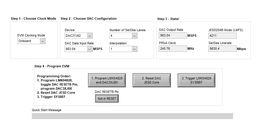
The DAC37J82 is set up in 4-2-1-1 mode and with K = 32.

The config for both the LMK04828 and DAC37J82 is attached. I'm evaluating deterministic latency and would like some help validating my config file, especially the SYSREF timing part. This way when I need to troubleshoot deterministic latency, I would at least eliminate the concern about SYSREF timing, at least for the LMK04828 and DAC37J82, since I have actual tuned setting from the TI team.

Thank you very much

Tyler

test.cfg

  • Hi Tyler,

    The particular test mode that you had posted above was verified on the TSW14J56 + DAC37j84 EVM. The release buffer delay (RBD) and the SYSREF setup/hold time are dependent on your FPGA design/delay/PCB board layout to the DAC37j84. It is possible that you have to re-tune this again.

    For details and guidelines, refer to following app note:

    http://www.ti.com/lit/an/slyt628/slyt628.pdf

  • Hi,

    Thanks for the response. I can tune the SYSREF timing to the FPGA and variables that are related to the FPGA hardware path.

    Can you help verify the SYSREF timing between the LMK04828 and the DAC37J82EVM and give me the optimized setting? This path is TI specific and not related to the variation in the FPGA hardware.

    Thanks,

    Tyler

  • Let me rephrase that to prevent misunderstanding.

    The SYSREF timing between the LMK04828 and the DAC37J82 on the DAC37J82EVM board, TI evaluation board.

    Thanks,

    Tyler

  • Hi Tyler,

    I am missing your concern, sorry.

    The DAC37j84 itself has SYSREF setup/hold time requirement of 50ps/50ps. The current LMK04828 and DAC37j84EVM are meeting this. All traces of CLK and SYSREF of the LMK04828 o the DAC37j84 are length matched to ensure the timing requirement.

    Perhaps there are some application specific questions on your side that require additional attention. Please clarify.

    -Kang

  • Hi Kang,

    Just to summarize our conversation. Per your analysis of my clocking configuration and the shared config setting, the SYSREF timing between the LMK04828 and the DAC37J82 on the EVM under the described config is solid and that there should be no further need from our team to tune any phase adjustment on this path. Which means that if we're trying to tune for deterministic latency, we have to look elsewhere and at other variables. Did I state your assessment correctly?

    Thanks,

    Tyler

  • Tyler,

    If you are talking about making sure the exact timing optimal on the LMK04828 side, you have to post this on the clock team E2E to have their recommendation. We can check functionality, but you need to get their blessing on this.

    Different settings of the LMK0428 will have different SYSREF response. You may see the app note below for detail:

    There are also many knobs to tweak for deterministic latency, which is highly dependent on your own PCB design. 

    From TI's perspective, the SYSREF/Clock timing was check on this particular EVM design (with the TSW14J56). You still have to do your own homework to check as well (Sorry, I have to refer you to the disclaimer below) Keep in mind JESD204 link is referenced to both FPGA and DAC, not just one side. Just because one side is tuned doesn't mean the other side is tuned. 

    IMPORTANT NOTICE AND DISCLAIMER

    TI PROVIDES TECHNICAL AND RELIABILITY DATA (INCLUDING DATASHEETS), DESIGN RESOURCES (INCLUDING REFERENCE DESIGNS), APPLICATION OR OTHER DESIGN ADVICE, WEB TOOLS, SAFETY INFORMATION, AND OTHER RESOURCES “AS IS” AND WITH ALL FAULTS, AND DISCLAIMS ALL WARRANTIES, EXPRESS AND IMPLIED, INCLUDING WITHOUT LIMITATION ANY IMPLIED WARRANTIES OF MERCHANTABILITY, FITNESS FOR A PARTICULAR PURPOSE OR NON-INFRINGEMENT OF THIRD PARTY INTELLECTUAL PROPERTY RIGHTS.

    These resources are intended for skilled developers designing with TI products. You are solely responsible for (1) selecting the appropriate TI products for your application, (2) designing, validating and testing your application, and (3) ensuring your application meets applicable standards, and any other safety, security, or other requirements. These resources are subject to change without notice. TI grants you permission to use these resources only for development of an application that uses the TI products described in the resource. Other reproduction and display of these resources is prohibited. No license is granted to any other TI intellectual property right or to any third party intellectual property right. TI disclaims responsibility for, and you will fully indemnify TI and its representatives against, any claims, damages, costs, losses, and liabilities arising out of your use of these resources. TI’s products are provided subject to TI’s Terms of Sale (www.ti.com/legal/termsofsale.html) or other applicable terms available either on ti.com or provided in conjunction with such TI products. TI’s provision of these resources does not expand or otherwise alter TI’s applicable

    warranties or warranty disclaimers for TI products.

    Mailing Address: Texas Instruments, Post Office Box 655303, Dallas, Texas 75265

    Copyright © 2019, Texas Instruments Incorporated