This thread has been locked.

If you have a related question, please click the "Ask a related question" button in the top right corner. The newly created question will be automatically linked to this question.

DAC39J84: DAC39J84 4421 configuration issues

Part Number: DAC39J84

Hi all,

I'm trying to get the DAC39J84 to work into 4421 configuration. However after configuring the device and start up the JESD links I got no data at the analog outputs.

After configuration I can verify that the active SERDES do not have errors (registers 0x64 to 0x68) and I can see in signal tap that the JESD links have been initialized properly:

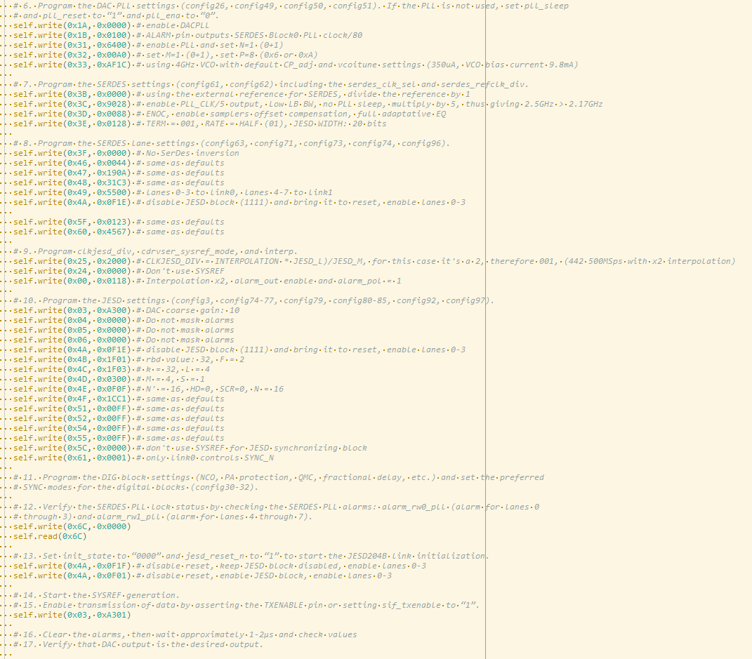
The configuration setup is as follows:

I really don't know what I'm doing wrong. Probably is something reasonably simple.

Thanks in advance.

dac39j84_dump.txt
DAC39J84 configuration
JESD settings: 4421
Fin = Fs: 500MHz, interpolation x2
DACPLL enabled, N = 1, M = 1, P = 8, VCO @ 4GHz
SERDES: 5Gbps, half rate PLL @ 2.5GHz

Read 0X118 from DAC39J84::0X0000
Read 0X03 from DAC39J84::0X0001
Read 0X2002 from DAC39J84::0X0002
Read 0XA301 from DAC39J84::0X0003
Read 0X00 from DAC39J84::0X0004
Read 0X00 from DAC39J84::0X0005
Read 0X00 from DAC39J84::0X0006
Read 0X2501 from DAC39J84::0X0007
Read 0X00 from DAC39J84::0X0008
Read 0X00 from DAC39J84::0X0009
Read 0X00 from DAC39J84::0X000A
Read 0X00 from DAC39J84::0X000B
Read 0X400 from DAC39J84::0X000C
Read 0X400 from DAC39J84::0X000D
Read 0X400 from DAC39J84::0X000E
Read 0X400 from DAC39J84::0X000F
Read 0X00 from DAC39J84::0X0010
Read 0X00 from DAC39J84::0X0011
Read 0X00 from DAC39J84::0X0012
Read 0X00 from DAC39J84::0X0013
Read 0X00 from DAC39J84::0X0014
Read 0X00 from DAC39J84::0X0015
Read 0X00 from DAC39J84::0X0016
Read 0X00 from DAC39J84::0X0017
Read 0X00 from DAC39J84::0X0018
Read 0X00 from DAC39J84::0X0019
Read 0X00 from DAC39J84::0X001A
Read 0X100 from DAC39J84::0X001B
Read 0X00 from DAC39J84::0X001C
Read 0X00 from DAC39J84::0X001D
Read 0X1111 from DAC39J84::0X001E
Read 0X1140 from DAC39J84::0X001F
Read 0X00 from DAC39J84::0X0020
Read 0X00 from DAC39J84::0X0021
Read 0X1B1B from DAC39J84::0X0022
Read 0XFFFF from DAC39J84::0X0023
Read 0X00 from DAC39J84::0X0024
Read 0X2000 from DAC39J84::0X0025
Read 0X00 from DAC39J84::0X0026
Read 0X00 from DAC39J84::0X0027
Read 0X03 from DAC39J84::0X0028
Read 0XFFFF from DAC39J84::0X0029
Read 0X00 from DAC39J84::0X002A
Read 0X00 from DAC39J84::0X002B
Read 0X00 from DAC39J84::0X002C
Read 0X00 from DAC39J84::0X002D
Read 0XFFFF from DAC39J84::0X002E
Read 0X04 from DAC39J84::0X002F
Read 0X00 from DAC39J84::0X0030
Read 0X6404 from DAC39J84::0X0031
Read 0XA0 from DAC39J84::0X0032
Read 0XAF1C from DAC39J84::0X0033
Read 0X00 from DAC39J84::0X0034
Read 0X00 from DAC39J84::0X0035
Read 0X00 from DAC39J84::0X0036
Read 0X00 from DAC39J84::0X0037
Read 0X00 from DAC39J84::0X0038
Read 0X00 from DAC39J84::0X0039
Read 0X00 from DAC39J84::0X003A
Read 0X00 from DAC39J84::0X003B
Read 0X9028 from DAC39J84::0X003C
Read 0X88 from DAC39J84::0X003D
Read 0X128 from DAC39J84::0X003E
Read 0X00 from DAC39J84::0X003F
Read 0X00 from DAC39J84::0X0040
Read 0X00 from DAC39J84::0X0041
Read 0X00 from DAC39J84::0X0042
Read 0X00 from DAC39J84::0X0043
Read 0X00 from DAC39J84::0X0044
Read 0X00 from DAC39J84::0X0045
Read 0X44 from DAC39J84::0X0046
Read 0X190A from DAC39J84::0X0047
Read 0X31C3 from DAC39J84::0X0048
Read 0X5500 from DAC39J84::0X0049
Read 0XF01 from DAC39J84::0X004A
Read 0X1F01 from DAC39J84::0X004B
Read 0X1F03 from DAC39J84::0X004C
Read 0X300 from DAC39J84::0X004D
Read 0XF0F from DAC39J84::0X004E
Read 0X1CC1 from DAC39J84::0X004F
Read 0X00 from DAC39J84::0X0050
Read 0XFF from DAC39J84::0X0051
Read 0XFF from DAC39J84::0X0052
Read 0X00 from DAC39J84::0X0053
Read 0XFF from DAC39J84::0X0054
Read 0XFF from DAC39J84::0X0055
Read 0X00 from DAC39J84::0X0056
Read 0XFF from DAC39J84::0X0057
Read 0XFF from DAC39J84::0X0058
Read 0X00 from DAC39J84::0X0059
Read 0XFF from DAC39J84::0X005A
Read 0XFF from DAC39J84::0X005B
Read 0X00 from DAC39J84::0X005C
Read 0X00 from DAC39J84::0X005D
Read 0X00 from DAC39J84::0X005E
Read 0X123 from DAC39J84::0X005F
Read 0X4567 from DAC39J84::0X0060
Read 0X01 from DAC39J84::0X0061
Read 0X00 from DAC39J84::0X0062
Read 0X00 from DAC39J84::0X0063
Read 0X00 from DAC39J84::0X0064
Read 0X00 from DAC39J84::0X0065
Read 0X00 from DAC39J84::0X0066
Read 0X00 from DAC39J84::0X0067
Read 0XA802 from DAC39J84::0X0068
Read 0XFF0F from DAC39J84::0X0069
Read 0XFF0F from DAC39J84::0X006A
Read 0X7C03 from DAC39J84::0X006B
Read 0X06 from DAC39J84::0X006C
Read 0X90 from DAC39J84::0X006D
Read 0X00 from DAC39J84::0X006E
Read 0X00 from DAC39J84::0X006F
Read 0X00 from DAC39J84::0X0070
Read 0X00 from DAC39J84::0X0071
Read 0X00 from DAC39J84::0X0072
Read 0X00 from DAC39J84::0X0073
Read 0X00 from DAC39J84::0X0074
Read 0X00 from DAC39J84::0X0075
Read 0X00 from DAC39J84::0X0076
Read 0X00 from DAC39J84::0X0077
Read 0X00 from DAC39J84::0X0078
Read 0X00 from DAC39J84::0X0079
Read 0X00 from DAC39J84::0X007A
Read 0X00 from DAC39J84::0X007B
Read 0X00 from DAC39J84::0X007C
Read 0X00 from DAC39J84::0X007D
Read 0X00 from DAC39J84::0X007E
Read 0X800A from DAC39J84::0X007F

  • Hi again, for some reason the image with the configuration setup didn't load properly. Here it is. Another thing I forgot to mention but I think it's obvious, is that the DACCLK and the SYSREF are present from the very beginning.

  • Javier,

    According to your settings, it appears you are using a 500MHz reference clock for the DAC PLL to generate a 500MHz DAC clk? Why are you doing this? Did you set the VCO tune so that the PLL was locked?

    With your settings, I was able to get an output with the TI DAC EVM using an external 500MHz reference clock. The configuration file is attached. 

    Regards,

    Jim

    DAC39J84_4421.cfg

  • Hi Jim,

    Thanks for the fast reply!

    I'm using the PLL as an easy way to check that I get a clock to the device, but yes it can be disabled. The DACPLL is locked (bit 0 at register 0x6C is 0).

    About the unused lanes. Should I keep them like that (sending comma chars indefinitely)?

    I'll check out your configuration to see if that works for us.

    Thanks

  • Javier,

    You can keep send comma chars on unused lanes. The DAC will ignore these. An easier way to verify if the DAC is getting a valid clock is to operate the part in NCO only mode. 

    Regards,

    Jim

    1325.DAC38RF82_NCO_CW.pptx

  • Hi Jim,

    It seems the configuration you sent me worked and we can see signals at the output.

    This is a bit off the topic but we see that the DAC introcudes overshoot/undershoot whenever tha sample is updated/changed so the signal looks quite bad. It can be easily filtered out but I believe the DAC should behave. The board uses the output circuit depicted at the DAC39j84 datasheet (page 77) with a TC1-1-13M+ balun from Mini-Circuits.

    I suspect of an impedance missmatch of some kind causing this effect, but I could use some advice from you.

    Kind regards


  • Javier,

    Is there a chance the data samples are out of order coming out of the FPGA? See attached file of what I think is your data sent to the DAC with my setup.

    Regards,

    Jim

  • Hi Jim,

    Could you elaborate a bit more about this? Maybe I'm missing something here...

    Data is fed from an FPGA based 16b NCO (IP generated). We byte swap the samples since for 442 MSB is sent first. I don't see a way that data is out of order (in 442 mode each lane feeds a DAC). On top of that we have seen the same behaviour on 841 mode.

    Thanks

  • Javier,

    Each lane is sending data to a converter. If the samples came out as 2,1,4,3,6,5,.... instead of 1,2,3,4,5,6,... you would see what you are observing I think.

    Regards,

    Jim

  • Hi Jim,

    I've analyzed the samples with signal tap, moved them to excel, plot them and they show a nice and clean sinewave.

    On the other hand, if you look at the first picture I sent you, the perturbance is exactly at Fs. If the samples were not ordered as you suggest, then the perturbance would be, at least, at twice the sampling frequency.

    You can count the peaks within a horizontal division, they are exectly 5 max and 5 min, with 5 samples every horizontal division (10 ns) running at 500MSps.

    Cheers

  • Javier,

    I am assuming this is a custom board. Can you send us your schematics? Can you also explain the last two scope screen shots you sent. Not sure what the second screen shot was showing.

    Can you try generating a tone that is the same frequency as the one from the FPGA data using the DAC internal NCO only and see how this output compares to the FPGA data? This should tell us if it is a board issue or not.

    Regards,

    Jim

  • Hi Jim,

    Yes, this is a custom board. It's a FMC231 from Vadatech (AC coupled outputs). Unfortunately I got no schematics, just a very simple block diagram with the clocking network. The images I've sent are as follows:

    The first image is a 20MHz sinewave from the FPGA using a IP-based NCO. The scope shows two DAC channels working on 442 mode with 500MSps (x2 interpolation).

    The second image is the same but one of the outputs (yellow) has been filtered with an external RF low pass filter. This image also shows an FFT plot but I don't think it's relevant. The FFT shows a 20MHz peak with two tones at 500+/-20 MHz. I personally think that's an artifact and not a real mixing.

    I'll try the NCO only mode. Can the DAC39J84 work without an incoming signal? I've look at the datasheet and it's only suppossed to mix the NCO, so I'll be driving a constant value at the DAC, so the NCO is mixed with something different than 0. Otherwise please let me know.

    Cheers and thanks for your help!

  • Hi Jim,

    We tested the NCO only mode (NCO in fine tune and SIFDAC value) and still shows the same behavior...

    Cheers

  • Javier,

    Attached are plots with our EVM using both the NCO and the FPGA to generate the 20MHz output. If you are not seeing this, I think there is an issue with the DAC output circuit you are using.

    You need to make sure the voltage on the IOUTP/N pins do not exceed the max compliance voltage of 0.6V and that the full scale output current does not exceed 30mA or you will see increased signal distortion. What value are you using for the Rbias resistor? This is connected between pin G10 and GND.

    Regards,

    Jim

    20MHz NCO and FPGA Outputs.pptx

  • Hi Jim,

    I'm still surprised there is some distortion on your output. Not as bad as mine though. I used to work with the same chipset on the Abaco Systems FMC144 and FMC120 and I don't remember having these issues.

    We've risen a support ticket to the board manufacturer to see if we can figure out what is wrong.

    Thanks a lot for your constant and fast support. Pretty much appreciated!

    Kind regards