This thread has been locked.

If you have a related question, please click the "Ask a related question" button in the top right corner. The newly created question will be automatically linked to this question.

ADS7822: Wrong Clock diagram and data value

Part Number: ADS7822

Hi,

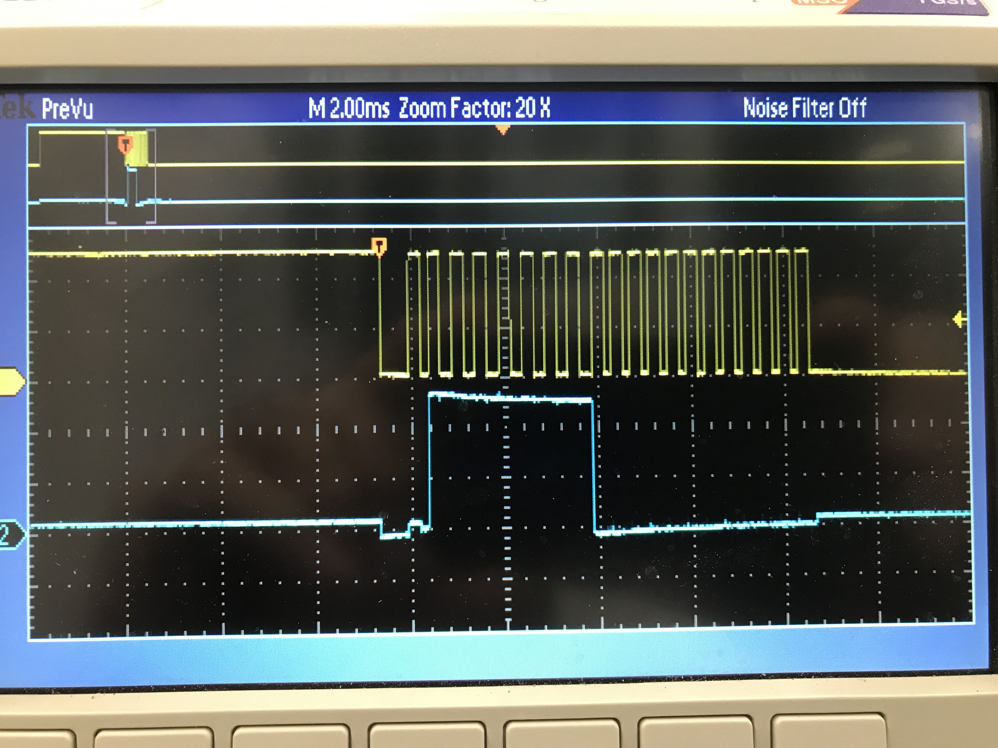
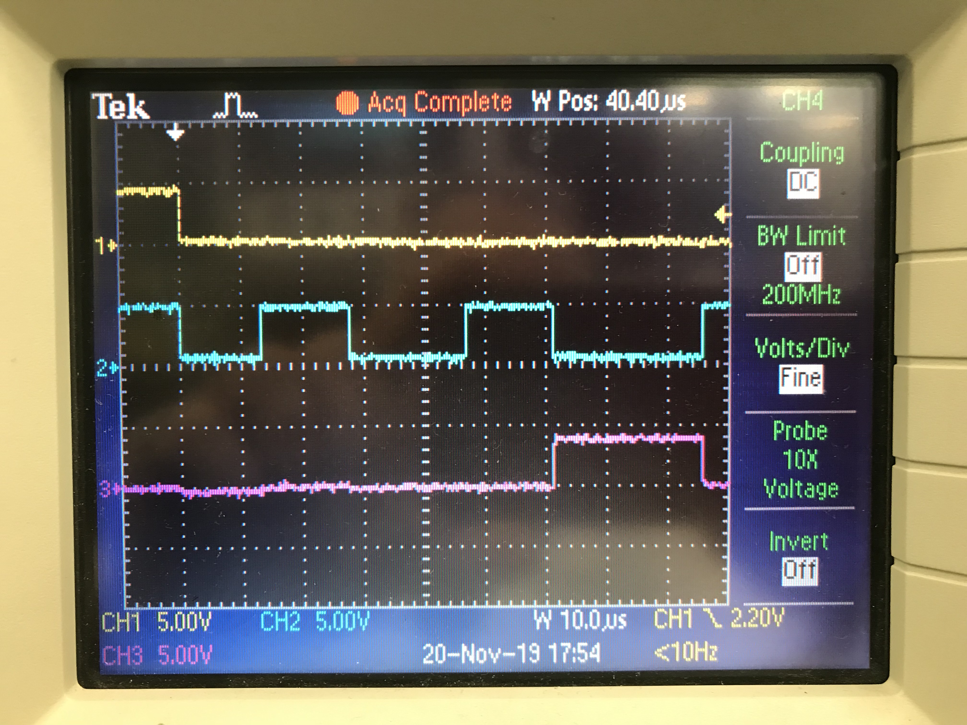
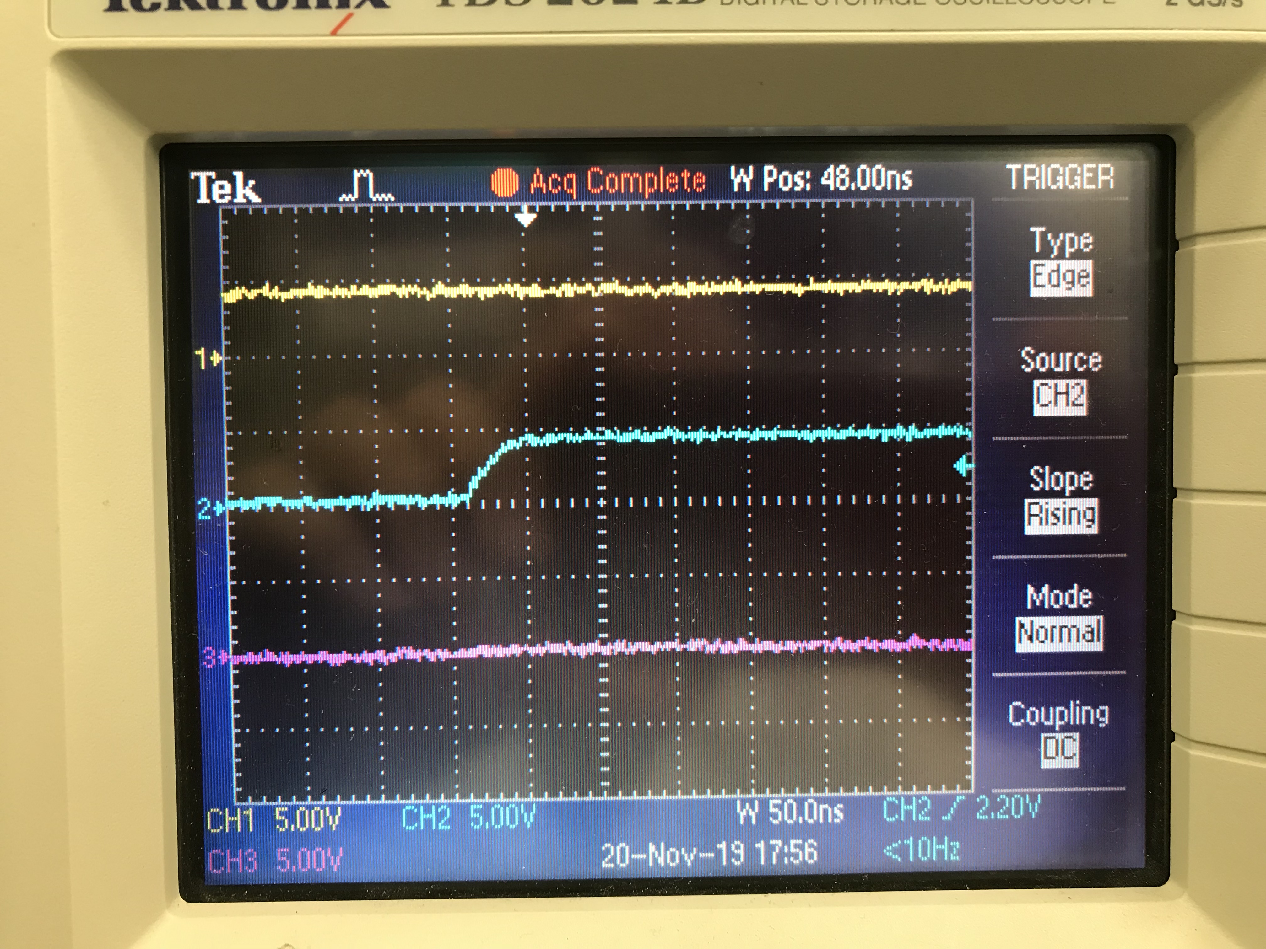
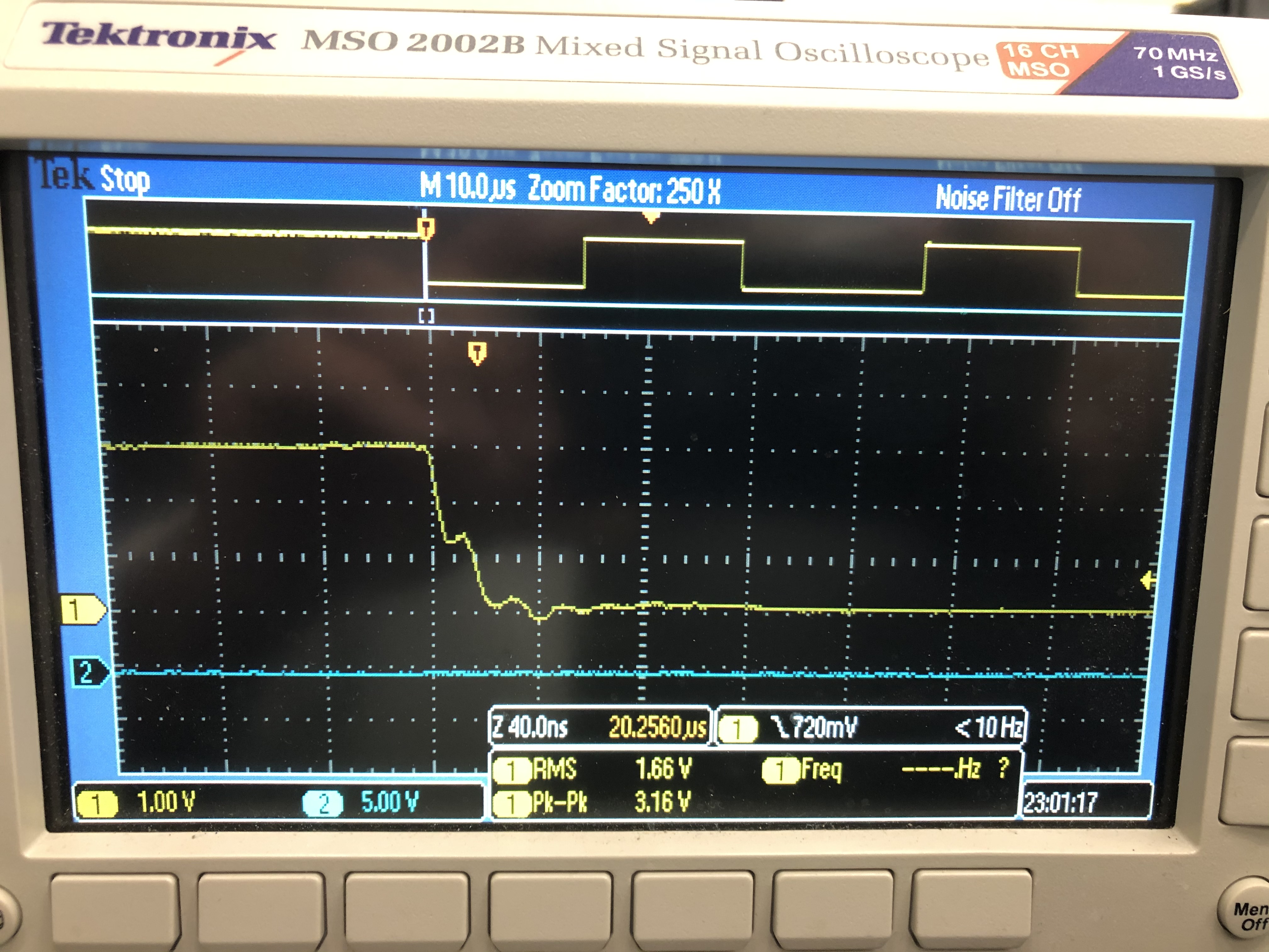
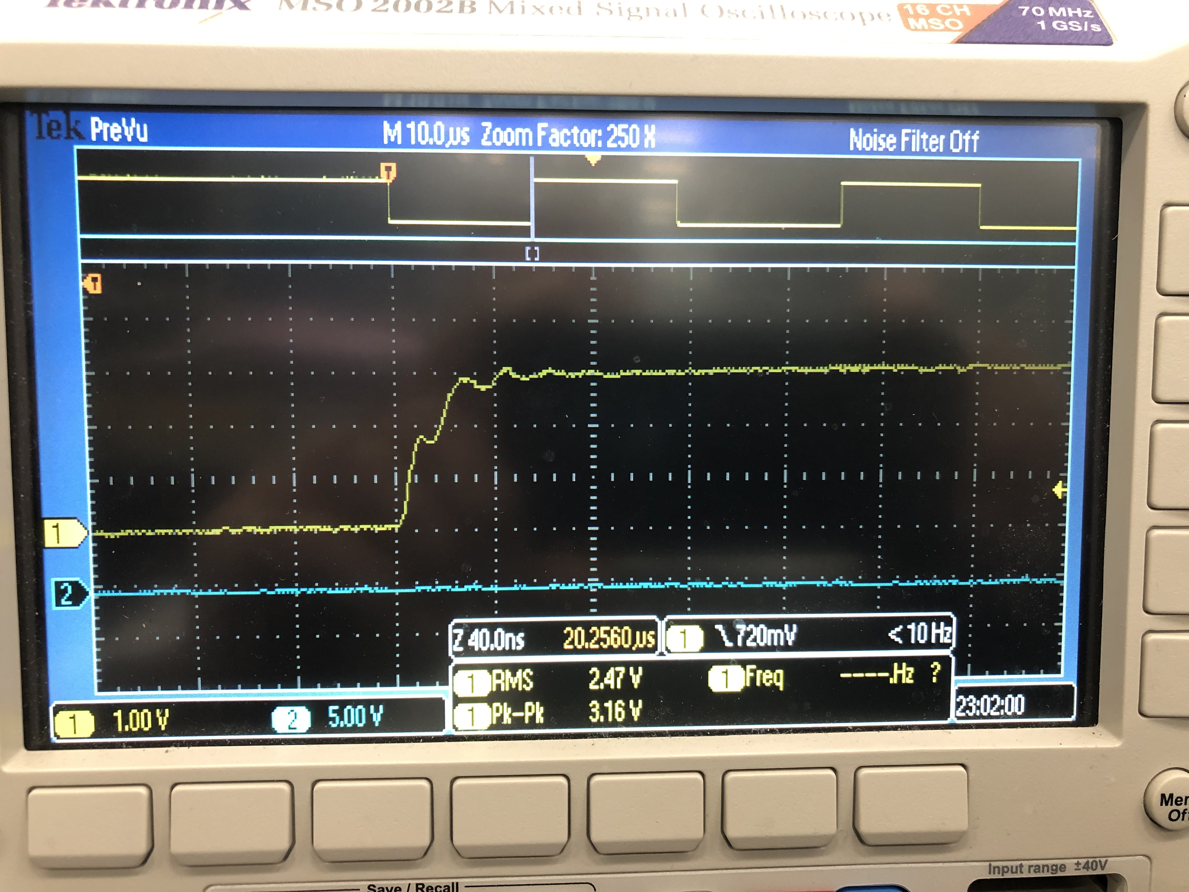
This chip does not behave at all as per its data sheet. The clocking diagram is not the same! The first two clock cycles conversion time are missing! Data line follows clock in some places and data received is NOT as per +IN and -IN analogue inputs. Please advise. Thanks.

M.A. 

  • Hello,

    Would you please share an oscilloscope shot with the digital lines probed, SCLK, CS, SDO

    This will help provide a visual check of the communication timing as well as confirming that what is actually happening matches was is expected from the firmware.

    I would also suggest using a known DC input for debugging, this way you know what to expect as our data measurements. For example, ground IN- and use a 2V input at IN+

    In your scope shots please describe what you mean by the first two clock cycles are missing.

    Note that this device has 2 clock cycles as the sample time, during this time SDO is still in HighZ state, and will not show valid data until after.  One full conversion requires 14 clock cycles.

    Regards

    Cynthia

  • Cynthia said:

    Hello,

    Would you please share an oscilloscope shot with the digital lines probed, SCLK, CS, SDO

    This will help provide a visual check of the communication timing as well as confirming that what is actually happening matches was is expected from the firmware.

    I would also suggest using a known DC input for debugging, this way you know what to expect as our data measurements. For example, ground IN- and use a 2V input at IN+

    In your scope shots please describe what you mean by the first two clock cycles are missing.

    Note that this device has 2 clock cycles as the sample time, during this time SDO is still in HighZ state, and will not show valid data until after.  One full conversion requires 14 clock cycles.

    Regards

    Cynthia

    Hi,

    Here are Scope shots. Because I had only two channel scope, you are not able to see CS line. However CS line is synchronized with the first CLK falling edge at the beginning. As seen in the first picture, the two first CLKs are missing during sampling time and you can ONLY see NUL bit instead on the first Clock. And why Data line is following clock on the second CLK? The other issue is that: as per data sheet, while CS is still low any CLK beyond 15 MUST display B0...B12 and this is not happening (third picture)?! The reading value of ADC is supposed to be 0.8VDC and it's totally off (First picture).

    Thanks,

    M.A.

  • Hi,

    Any update on this?

    Thanks,

    M.A.

  • Hello,

    Apologies on the late response

    The data transfer should occur on the falling edge of SCLK.

    Is there anything else on the communications lines? what does your set up consist of? are there many blue wires and long connections?

    Please make sure the CS and SCLK meet timing requirements. SCLK needs to rise within 1000us of CS falling. I cannot see CS in this scope, but assuming that SCLK goes low when CS goes low, this requirement is not being met.

    What is your clock source? Is this a clean signal, it seems to be a bit uneven in the scope.

  • Hi,

    Thanks for the response.

    CS, SCLK and Data lines are buffered. So long connection does not matter. What is "blue wire" you mentioned? I have attached the schematic for you. Note that Scope probing is just at the ADS7822 chip.

    I have attached better Scope pictures with CS line visible. CLK timing is as per data sheet. CLK is not even because is driven by MCU and is programmable. That should not matter if duty cycle is variable as per data sheet. I have included also CLK rise time picture. Rise time is under 50 ns.

    Everything as per data sheet and yet the result is NOT! I believe, there is definite problem with the chip. Attached picture timing diagrams do not correspond to its data sheet. That is:

    1.  1 1/2 Sampling clock cycles are missing and only NULL bit clock is present. Because of this the reading is off!

    2. In the timing diagram, in some places, Data line follows CLK line that is very odd! This has been brought up in other forum as well.

    3. If CLK continues to be present after 15 CLKs, Data will NOT be present as suggested in the data sheet.

    Please advise.

    Thanks,

    M.A.

  • This is odd behavior.

    By blue wiring I mean having lose wires make connections on a PCB. This are changes and edits that have to be done after the PCB is manufactured by using physical wires to make connections.

    The digital isolator does not seem to be grounded properly from your schematic. I would suggest making sure that is properly grounded and powered.

    There could be ringing that is causing double clocking causing the SDO to behave oddly.

    If you would like to narrow the source of the issue to either the board or the device. You can move the device to a working board and see if the issue follows the deice. You can also use a new device that has proven to work correctly and place on the not working board and see the if the issue is still present.

    Regards

    Cynthia

  • Hi,

    Yes, I do have a lot of blue wires. The PCB is tested in a fixture with lots of probes (pogo pins) and long connecting wires. And seems to be a problem on the CLK line.

    I replace the device but the problem existed. I tested the device with shorter wire and no probing and it did work. I narrowed the problem to CLK while probing in the system. I think, the problem is that: CLK rise and fall time has some staggering steps. Data sheet does NOT specify at all about CLK rise and fall time ALONE. Looks like, this device is very sensitive to CLK and any ringing or reflection is causing erroneous internal latches!

    My other observation is that, as opposed to data sheet the null bit is missing. This means, after two clock cycle data is ready as opposed to three. This fact makes it a lot difficult for the programmer to synchronize this device. I guess, operation of chip entirely with CLK line has its own disadvantage!

    Thanks for the support.

    Regards,

    M.A.