This thread has been locked.

If you have a related question, please click the "Ask a related question" button in the top right corner. The newly created question will be automatically linked to this question.

TSW54J60EVM: 8-2-2-4 Configuration Setting and with FOVR enabled

Part Number: TSW54J60EVM
Other Parts Discussed in Thread: ADS54J60

Hi,

I'm currently using 8-2-2-4 mode with the attached configuration setting and would like some help addressing two questions.

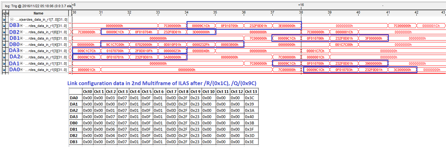
1. Is my configuration setting right for 8-2-2-4? I'm using the local onboard oscillator as reference clock.

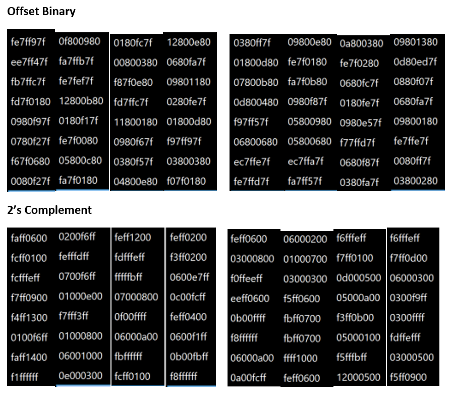
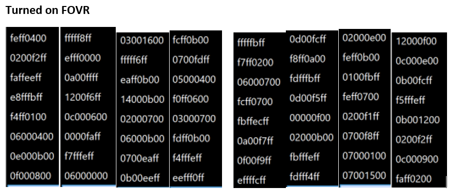
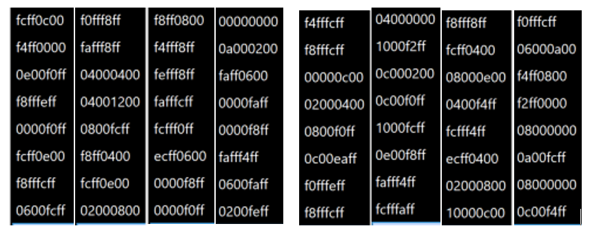
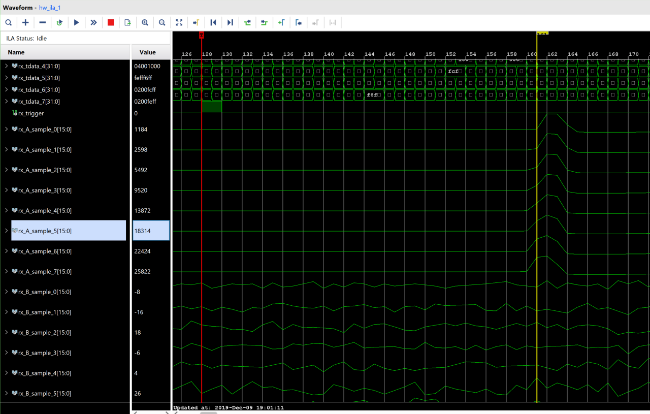
2. On the FPGA side my parallel data bus at the other end of the 8-lane JESD204B interface is 256-bit, 32-bit per lane. I'm currently trying to figure out how the 16-bit samples from both channel A and B are supposed to be showing up. I'm currently assuming that for every 32-bit per lane, the samples are aligned on 16-bit boundary so basically one sample would be in bits 31-16 and another sample would be in bits 15-0. Is this assumption correct? Also I tried to turn on FOVR to force the LSB to 0 if my input signals are low and below the FOVR range so that this can help give more insights on any other potential byte-swap in the data representation but with 16-bit boundary assumption, this is not working and I don't know if it's alignment or if the FOVR setup is not working.

Thanks in advance for the help,

Tyler

ADS54J60.cfg

  • Tyler,

    With register 0x680043 set to 0x00, the output data format is 2's comp. Your notes say "Offset Binary".

    You do not program the FOVR threshold but the default is set to 0xE3.

    Make sure you toggle the board reset after power and clocks are applied and before you load the registers.

    Your sample assumption is correct. What FPGA are you interfacing this EVM with? Have you verified that link gets established and SYNC goes high?

    Regards,

    Jim

  • Hi Jim,

    I'm flipping the data format bit in the configuration file to look at data in both 2's complement and offset binary format. I also do use the power reset button on the board.

    I'm interfacing this with a Kintex Ultrascale Xilinx FPGA. On the FPGA side, 8-lane link were established and SYNC is high. Status on the FPGA side also reports proper link configuration parameters and I did notice data started to transition from all 0s after link was established.

    Below you can see a screenshot of a couple of data blocks in both offset binary and 2's complement format. This data was collected with FOVR turned off.

    And below is a screen shot of data patterns in 2's complement mode after FOVR is turned on.

    Since the data in the first screenshot doesn't quite reflect the ADC input state of a low signal. I tried to use FOVR as a test to confirm whether the parallel data really does reflect the ADC input states. The FOVR range is high enough by default so I didn't try to change it as my input signal is low. I'm expecting the LSB in the samples to be 0 but the data doesn't support this.

    Now I'm focusing on getting FOVR to work first and trying to figure out why this is not working.

    Thanks for the help,

    Tyler

  • Tyler,

    Using your settings I was able to get the FOVR to toggle on CHA LSB. When I input a 10MHz tone at -3dBm, the LSB is a solid "0". With the power changed to -2dBm, the LSB starts to toggle.

    Regards,

    Jim

  • E2E_ADS54J60_LMF_8224.cfgTyler,

    There is one mistake with your config file. You must do the digital reset before loading the other registers in page 0x68. Otherwise, it will reset your settings.

    See attached file.

    Regards,

    Jim


  • Hi Jim,

    Thanks for the modified config file. I have tried this modified config and below is a screen shot of 2 blocks of multi-frames. The 1s in the LSBs are still there so this tells me FOVR is still not working quite right so I have to keep troubleshooting this FOVR setup.

    On another note, I also attached a figure from the datasheet of the ADS54J60 below. In 8-2-2-4 mode, and since each chunk of my data has 2 frames in it instead of 1, thus I'd be expecting 8 samples from both channels. Is it safe to assume as followed the sequence of samples?

    A3[15:8]  A3[7:0]  A7[15:8]  A7[7:0]  (each 32-bit per lane)

    A2[15:8]  A2[7:0]  A6[15:8]  A6[7:0]

    A0[15:8]  A0[7:0]  A4[15:8]  A4[7:0]

    A1[15:8]  A1[7:0]  A5[15:8]  A5[7:0]

    B3[15:8]  B3[7:0]  B7[15:8]  B7[7:0]

    B2[15:8]  B2[7:0]  B6[15:8]  B6[7:0]

    B0[15:8]  B0[7:0]  B4[15:8]  B4[7:0]

    B1[15:8]  B1[7:0]  B5[15:8]  B5[7:0]

    Thanks,

    Tyler

  • Re-posting the 2 screenshots for my previous reply. They somehow did not show up after the post.

    Thanks,

    Tyler

  •  Tyler,

    This is correct. Instead of observing the FOVR, why don't you try looking at the ILA data. This may be more helpful with trying to figure out if there is some type of octet swapping issue. See the attached slide for an example of ILA data capture from an ADS54J60 using Altera's Signal Tap tool.

    Regards,

    Jim

  • Hi Jim,

    I did figure out the order of the octets and also the sequence of the 8 16-bit samples from lane to lane yesterday but wanted to make an FPGA build with all the re-ordering hooks in place to look at a proper signal pulse and check for conversion representations to make sure that it is not just speculation. I haven't tried looking at the ILA sequence as you mentioned and I'll keep this in mind.

    Using FOVR information to force the LSBs to 0, I did notice 2 out of the 4 octets always had their LSBs stuck to 0 and they were byte 1 and byte 3 from within a 32-bit word. This tells that byte 0 and byte 0 and byte 2 have the upper [15:8] information of the 16-bit data samples. Please see below for the screenshot of the capture of a 20-ns pulse width signal with the reordering of the octets from within a 32-bit word and also the sequence of the 8 samples from lane to lane. What's mentioned in the datasheet is only part of the story.


    I used FOVR to force the LSBs to 0 to help troubleshoot octet alignment issues. This is step 1 and for step 2, I need to use it to evaluate deterministic latency because it does have better detection resolution.

    Currently I'm injecting a pulse into the board and using digital means to detect the rising edge of the signal by using one of the upper MSB bits of the data to trigger on a certain threshold. I have at most 8ns detection resolution from within a cycle @125Mhz in 8-2-2-4 mode and at most +/- 1ns adding taking into account the position of the trigger from within the 8-sample window. I want to understand more about the FOVR detection capability to see if I can get better detection resolution using this method. Here are my follow-up questions.

    1. I want to see the FOVR bit flipped to a '1' now and so I need to program the FOVR_THRESHOLD accordingly to catch the signal. Can you advise whether the following lines are correct to be added to my config file?

    ADS54Jxx_ANALOG

    0x0011 0x0F

    0x005F FOVR_THRESHOLD_VALUE

    2. Regarding the FOVR detection and I'm trying to understand detection resolution, Is the detection on the analog domain or on the digital domain by comparing converted samples? I want to see if using FOVR would actually allow me more detection resolution, better than if I was to do it on after the JESD link evaluating digital samples.

    Thanks,

    Tyler

  • Tyler,

    For #1, that is correct.

    For #2, I will have to check with the design team. 

    Regards,

    Jim