This thread has been locked.

If you have a related question, please click the "Ask a related question" button in the top right corner. The newly created question will be automatically linked to this question.

ADC12J1600: ADC12J1600: JESD204B data format and data mapping

Part Number: ADC12J1600

Hi,

I'm using ADC12J1600 to sample the data processed by KC705. I have some questions about the output data format of ADC12J1600. Since I'm setting the ADC to "decimation by 4" mode, I've learned about the data format of the DDC should be like this:

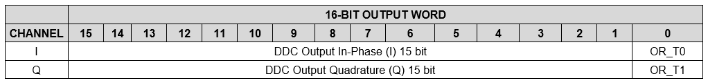
My question is, considering the raw sampled data of ADC12J1600 has 12bits, do all 15 bits here represent the value of data after decimation? Is one of the 15 bits the sign bit?

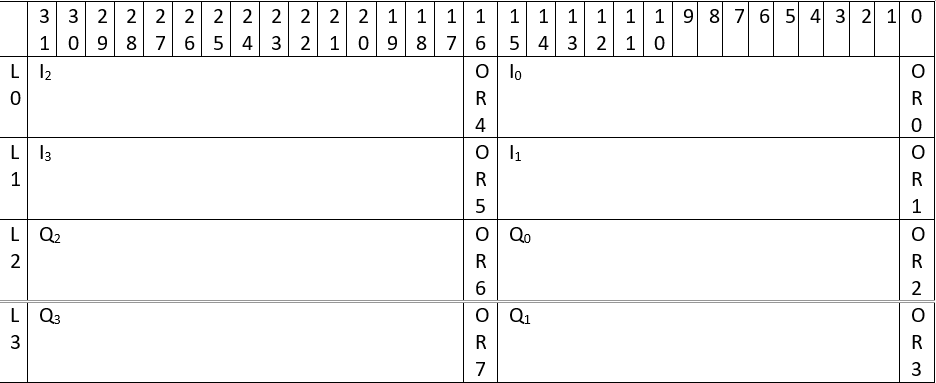
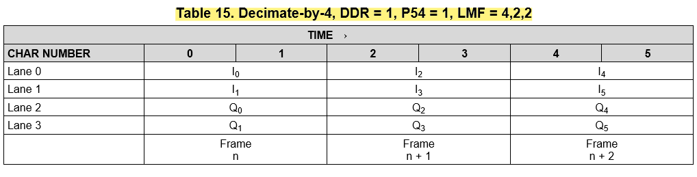
Another thing is, the parameters of the serial link I set should be LMFS = 4222. Here's the table about this:

I've downloaded the JESD204B demo project onto FPGA, and I've checked the data format of the receiver. The data of each lane has 32 bits. Could you provide some advice about data mapping here?

Thanks in advance for your help, I'm looking forward to your reply.

Best,

Haotian.

  • Haotian,

    All 15 bits represent the value of data. The data can either be offset binary or 2's comp. In the case of 2's comp, the MSB is the sign bit.

    The receiver is processing 32 bits per lane. This is a function of the Xilinx JESD204B IP. In 4222 mode, each lane is sending one complete sample every frame clock. Since there are two lanes for I data and 2 lanes for Q data, 2 complete samples of each will occur within a frame clock. The data will come out in two octets, with the first octet the MSB byte and the second octet as the LSB byte of the sample.

    The attached document may have information regarding your question.

    Regards,

    Jim

    1300.JESD204_TI_reference_design.pdf

  • Hi Jim

    Thanks for the response.

    Since you mentioned the data can be either offset binary or 2's complement, and I noticed on ADC12J1600 datasheet that decimated mode always output data in signed 2's complement. Is that always the case?

    For each 32-bit RX_data, I think the first 16 bits represent the first sample and the next 16 bits represent the second sample, am I right? Besides, you mentioned the data will come out in two octets, with the first octet the MSB byte and the second octet the LSB byte of the sample. Does it mean, the first and the second octet need to be switched to represent the real value of the sample?

    Thanks,

    Haotian.

  • Haotian,

    You are correct. In decimate mode, the ADC always outputs data in 2's comp mode. Regarding your other question, what are you trying to accomplish? The firmware used by the KC705 was designed to be used with HSDC Pro and is not recommended to be used for new designs. The user should go to the Xilinx website and use the examples provided. See comments on page 2 of the document I sent in the last post.

    Regards,

    Jim

  • Hi Jim

    Here is what I think about the data frame of JESD204B's receiver, I'm wondering if I'm understanding it in the right way:

     If I'm trying to get the value of each sample, can I directly ignore the two over-range threshold-detection control bits which, I think, should be bit[0] and bit[16] 

    Best,

    Haotian.