This thread has been locked.

If you have a related question, please click the "Ask a related question" button in the top right corner. The newly created question will be automatically linked to this question.

CCS / DAC8771: DAC8771 ???

Part Number: DAC8771
Other Parts Discussed in Thread: DAC8775

Tool/software: Code Composer Studio

Hello.
I am trying to set up a system using DAC8771. I made the electronic circuit according to EVM. I am sending data via SPI with STM32F407. However, the system does not work. The output voltage is always 0V. 
AVDD / PVDD 12V.
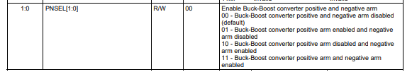
VNEG + 140mV and VPOS + 3.3V on the BBC. VREF is set to 5V.
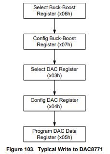
How to register. I tried to do it according to the datasheet but it does not happen. What should I do?
  • Hi,

    My colleague Reza will respond to this question today or Monday.

    Thanks,

    Paul

  • Murat,

    I would suggest that you share your schematic so we can double-check it. I see that you have based it on the EVM, but a review wouldn't hurt.

    Further details on how you are interacting with the device via SPI would also be helpful (i.e. SCLK phase / polarity settings, oscilloscope captures of a transfer to check logic levels, and the content of the SDI data you are writing / reading).

    Without such details we do not have much to go on right now. 

  • Thanks for the quick response. The scheme is this way. I have done many trials on SPI but the result has always been the same. 0V. I also tried different configurations for the BBC. But as I said, always VPOS = 3.3V
    VNEG = 0,15V
    At first I want to simply get the output value. I think if I can take different values ​​from zero, I will do the rest. For this, please tell me which register and which value will be written respectively..  Thanks

    DAC8771 AO.pdf

  • Murat,

    Your schematic around the DC/DC appears to be clean and the start-up values around 3.3V would make sense as well. Page 42 of the datasheet documents the high-level write sequence. I have pasted that graphic below.

    Essentially the process of configuring the DC/DC or DAC starts with a write to the "Select" register, this is to be compliant with the similar register format of the quad-channel DAC8775 sibling. So to configure the DC/DC one begins with a write to 0x06 and writing a 1 to bit 0 to select "Channel A". Following this, address 0x07 should be written with the desired DC/DC configuration - including enabling the "arms" of the DC/DC based on bits 0 and 1 in 0x07.

  • Thank you for your reply. 

    The issue has been resolved by following your explanation.

    Actually the datasheet caused a bit confusion regarding channel and DC/DC selection. The term "Channel A selected" is not clear at first to unfamiliar people. If there were a bit explanation what 0 mean and what 1 mean of that bit then it would not cause confusion. 

    Thank you again.

  • Murat,

    Thank you for the feedback. It's actually something we discussed internally a couple of days back as a number of folks seem to get hung up on this regarding both the DC/DC and the DAC itself. We will look at means to update the documentation and perhaps an additional section to make things as clear as possible.