This thread has been locked.

If you have a related question, please click the "Ask a related question" button in the top right corner. The newly created question will be automatically linked to this question.

ADS1261: Peer review of schematic and pseudo code

Part Number: ADS1261
Other Parts Discussed in Thread: TMUX1511, REF5050, , TPS7A47, TPS731

Dear Mr. Hall

Thank you for your help on this part in the past.  As I've mentioned before, I've made some design errors on this project.  After correcting the design errors, I'm ready to do another spin of this PCA.  I don't know if you guys at TI do this sort of thing but if you can, I would really appreciate a design review on the attached schematic and pseudo code.  My mistakes have already cost us a lot of money and I would like to avoid a repeat. 

A brief description: I'm using the TI reference "Using the ADS1261 Integrated AC Excitation Mode to Remove System Offset and Drift sbaa290" as a design guide.  I'm measuring three things; excitation current, bridge supply voltage and the bridge output voltage.  I'm using the 5vdc AVCC as a reference for the excitation current and bridge supply voltage measurements and the bridge supply voltage as a ratiometric reference for the bridge output voltage measurement.  Please see attached.  Any and all comments and corrections are very much appreciated.  Thank you.

Dennis_Test_2-2.pdfADS1261 Pseudo Code for AC Excitation.docx

  • Hi Dennis,

    Sure, I can review your schematic.

    One quick question though...what is the nominal bridge impedance? Is it a typically a 1kOhm load (with respect to the excitation source)?

    Here are my comments:

    • The AIN2 and AIN3 signals appear to be reversed...
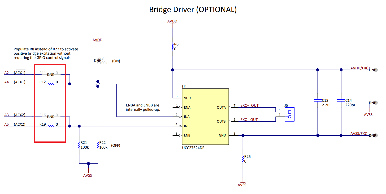
      The TMUX1511 will connect the source and drain pins only when the corresponding SEL pin is high (as controlled by !ACX1 and !ACX2 GPIO signals), and the +Bridge_EXC_1 and -Bridge_EXC_1 signals will get connected to either GND or AINCOM

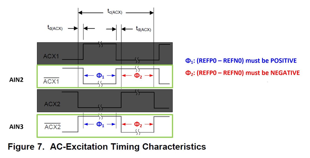
      Below is a diagram of the ac-excitation and what the ADS1261 expects in terms of reference voltage polarity...
      • In phase 1, !ACX2 will be high resulting in +Bridge_EXC_1 = GND and -Bridge_EXC_1 = AINCOM, so the reference voltage will appear to have a negative polarity to the ADS1261.


    • The AVSS and DGND pins appear to be missing a connection...
      In a unipolar supply configuration, the AVSS and DGND pins MUST be connected together (and ideally, would also share the same ground plane). 

    • I don't recommend using the REF5050 to power the ADS1261...
      The limited 10 mA output drive current of the REF5050 will not be sufficient and we've have seen performance issues with the ADC when the circuit is configured this way. I would recommend using an LDO that can supply at least 100 or 150 mA output current to power the ADC and bridge.

    • Avoid using inductors on IC supply pins...
      Inductors can choke the supply current to an IC and sometimes create performance issues (particularly with digital or mixed signal ICs that may have fast transient currents). Also, supply pins typically have large decoupling capacitors which may form an LC resonator and creates oscillates on the supply pin, instead of acting as a 2nd-order LPF.

    • Consider using a 5V supply as an excitation voltage for the bridge...
      You can typically use the AVDD supply for the ADC to also excite the bridge. The larger voltage drop across the bridge will provide a larger input voltage to the ADC and will likely improve sensitivity and resolution.
  • Dear Mr. Hall

    Thank you for your response.  To your points:

    One quick question though...what is the nominal bridge impedance? Is it a typically a 1kOhm load (with respect to the excitation source)?

    The bridge is a 3.5K bridge.  All for legs are 3.5K.  This of course is optimal.  The actual value is specified on the calibration sheet for each sensor.  These sensors are high precision sensors and a full calibration sheet come with each one. 

    The AIN2 and AIN3 signals appear to be reversed.

    Dam, I had it correct the first time.  When I reviewed my design, I think I misunderstood the timing, so I reversed the signals.  So I understand this correctly, when the AC Excitation starts, the !ACX1 goes low.  It doesn't start out high.

    The AVSS and DGND pins appear to be missing a connection.

    The AVSS and DGND pins are both connected to the same ground plane.

    I don't recommend using the REF5050 to power the ADS1261.

    I chose the REF5050 because of its accuracy and stability.  When I read the ADS1261 specifications, I thought the most it would draw would be about 7mA (see pg 10 of spec sheet).  How much do you believe the ADS1261 will draw?  Do you have a recommended LDO.  The PCA and sensor will be tested in an Environmental chamber that will be cycled between 15°C and 55°C.  I'm trying to design a data acquisition system that is very quiet and stable.

    Avoid using inductors on IC supply pins.

    I understand what you're saying.  I was advised to put the inductor in to help filter high frequency noise from two SMPS but in light of what you've said, I'll remove the inductors.

    Consider using a 5V supply as an excitation voltage for the bridge.

    Factory specifications call for a 1mA current drive if calibrated accuracy is to be maintained.  I understand the desire to have a greater dynamic range.  It's one of the things I try to maximize in my data acquisition systems.  However, the manufacturer has said that operating outside of their recommended limits will place the sensor in a nonlinear response. 

    Besides the hardware review, which I truly appreciate, what of my pseudo code?  Does it appear correct? 

  • Hi Dennis,

    Dennis McGlumphy said:

    One quick question though...what is the nominal bridge impedance? Is it a typically a 1kOhm load (with respect to the excitation source)?

    The bridge is a 3.5K bridge.  All for legs are 3.5K.  This of course is optimal.  The actual value is specified on the calibration sheet for each sensor.  These sensors are high precision sensors and a full calibration sheet come with each one. 

    OK, I was asking to know what to expect for a voltage drop across the bridge and to check if the ADS1261's IDAC compliance range would be exceeded (i.e. VAINCOM cannot exceed AVDD - 1.1V  for the IDAC to work). Since you have a 3.6 kOhm load on IDAC1, you have 0.3V of headroom.


    Dennis McGlumphy said:

    The AIN2 and AIN3 signals appear to be reversed.

    Dam, I had it correct the first time.  When I reviewed my design, I think I misunderstood the timing, so I reversed the signals.  So I understand this correctly, when the AC Excitation starts, the !ACX1 goes low.  It doesn't start out high.

    If there is any doubt of which signals to connect, you might consider adding resistors in front of the TMUX1511 to rewire the ACXn signals, if needed; similar to the options provided on the ADS1261EVM.


    Dennis McGlumphy said:

    I don't recommend using the REF5050 to power the ADS1261.

    I chose the REF5050 because of its accuracy and stability.  When I read the ADS1261 specifications, I thought the most it would draw would be about 7mA (see pg 10 of spec sheet).  How much do you believe the ADS1261 will draw?  Do you have a recommended LDO.  The PCA and sensor will be tested in an Environmental chamber that will be cycled between 15°C and 55°C.  I'm trying to design a data acquisition system that is very quiet and stable.

    The 7 mA is an average dc current draw, but digital transients can momentarily exceed 7mA. During power-up, for example, I've observed momentary current amplitudes of 50 mA or more.

    The ADS1261EVM used the low-noise TPS7A47, but I think any of the LDO's on this list would be fine: LDO parametric search results.


    Dennis McGlumphy said:

    Consider using a 5V supply as an excitation voltage for the bridge.

    Factory specifications call for a 1mA current drive if calibrated accuracy is to be maintained.  I understand the desire to have a greater dynamic range.  It's one of the things I try to maximize in my data acquisition systems.  However, the manufacturer has said that operating outside of their recommended limits will place the sensor in a nonlinear response. 

    Since the cell is specified to be used with a current excitation, I would stick with the IDAC excitation.

    I was expecting a 1kOhm nominal bridge impedance and only a 1V drop across the bridge. However, with a 3.5kOhm load and 1 mA excitation, you're closer to the maximum 5V reference input.


    Dennis McGlumphy said:
    Besides the hardware review, which I truly appreciate, what of my pseudo code?  Does it appear correct? 

    I don't see any issues with the pseudo code, just two quick comments on it though...

    • [General setup] Once you swap AIN2/AIN3, you'll probably want modify the default GPIO output levels so that AIN3 is set high.

    • [Measure excitation current] It is not a problem if you decide to use the analog supply as the reference source; however, since the IDAC current is derived from the internal reference you'll have a somewhat more ratiometric measurement if you use the internal reference source.

      Also, if for some reason the internal reference has not been enabled, you'll see the REFL_ALM when using the internal reference (when using the analog supply as the reference source, you will not see the REFL_ALM if the internal reference is off - but of course you would still see this error reflected in a near 0 mA current result).

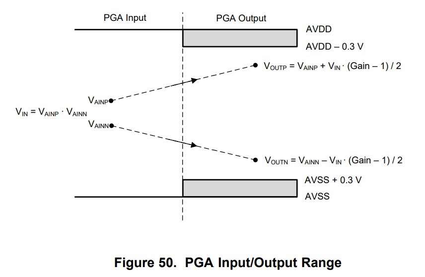
    One last thing I recommend checking, is to determine if there are any issues with the PGA input/output range...

    I don't know the maximum output voltage you expect to measure from the bridge, but you'll want to make sure that with the 16 V/V gain, that VOUTN (i.e the PGA negative output voltage, as indicated in the figure below) doesn't drop below AVSS + 0.3V and cause the PGA output to saturate. Since the common-mode output voltage of the bridge is biased closer to AVSS at 1.75V (3.5 kOhms * 1 mA / 2), there is not quite as much input swing range on the AVSS side, so as long as the PGA doesn't saturate on the AVSS side, you should have sufficient range on the AVDD side.

  • Dear Mr. Hall

    OK, I was asking to know what to expect for a voltage drop across the bridge and to check if the ADS1261's IDAC compliance range would be exceeded (i.e. VAINCOM cannot exceed AVDD - 1.1V  for the IDAC to work). Since you have a 3.6 kOhm load on IDAC1, you have 0.3V of headroom.

     Here is a more complete description of the pressure sensor.  The sensor is an absolute pressure sensor that has a range of 0 bar to 3 bar.  The bridge output at 0 bar is 0 volts and 140mv at 3 bar.  I've used the ADS1261 design tool to ensure the PGA output is within the bounds of the reference which should be in the range of 3.5 volts.  I believe this is OK.  Your thoughts please.

    If there is any doubt of which signals to connect, you might consider adding resistors in front of the TMUX1511 to rewire the ACXn signals, if needed; similar to the options provided on the ADS1261EVM.

    I think I've got everything understood considering the AC excitation connections.  But will take your advise anyway.

    The 7 mA is an average dc current draw, but digital transients can momentarily exceed 7mA. During power-up, for example, I've observed momentary current amplitudes of 50 mA or more.  The ADS1261EVM used the low-noise TPS7A47, but I think any of the LDO's on this list would be fine: LDO parametric search results.

    As I've said before, I'm trying to make a very quiet and accurate system.  The TPS7A47 is quiet enough but the accuracy (2.5%) is unacceptable and the specification sheet doesn't even list the TC.  I think I'll use the TPS731.  I've use it in the past and it worked out OK.  What are your thoughts on this regulator? 

    [Measure excitation current] It is not a problem if you decide to use the analog supply as the reference source; however, since the IDAC current is derived from the internal reference you'll have a somewhat more ratiometric measurement if you use the internal reference source.

    Will do.  I think using the internal reference will be better.  The input will be a greater percentage of the scale.  That should be better.  Is this correct thinking?

    I don't know the maximum output voltage you expect to measure from the bridge, but you'll want to make sure that with the 16 V/V gain, that VOUTN (i.e the PGA negative output voltage, as indicated in the figure below) doesn't drop below AVSS + 0.3V and cause the PGA output to saturate. Since the common-mode output voltage of the bridge is biased closer to AVSS at 1.75V (3.5 kOhms * 1 mA / 2), there is not quite as much input swing range on the AVSS side, so as long as the PGA doesn't saturate on the AVSS side, you should have sufficient range on the AVDD side.

    As I described the sensor above, please check to see if my calculations are correct and that I used the design tool correctly.  Thank you for all your help.