This thread has been locked.

If you have a related question, please click the "Ask a related question" button in the top right corner. The newly created question will be automatically linked to this question.

ADS1256: Seeing a lot of noise when reading small amplitude signals

Part Number: ADS1256

Hi,

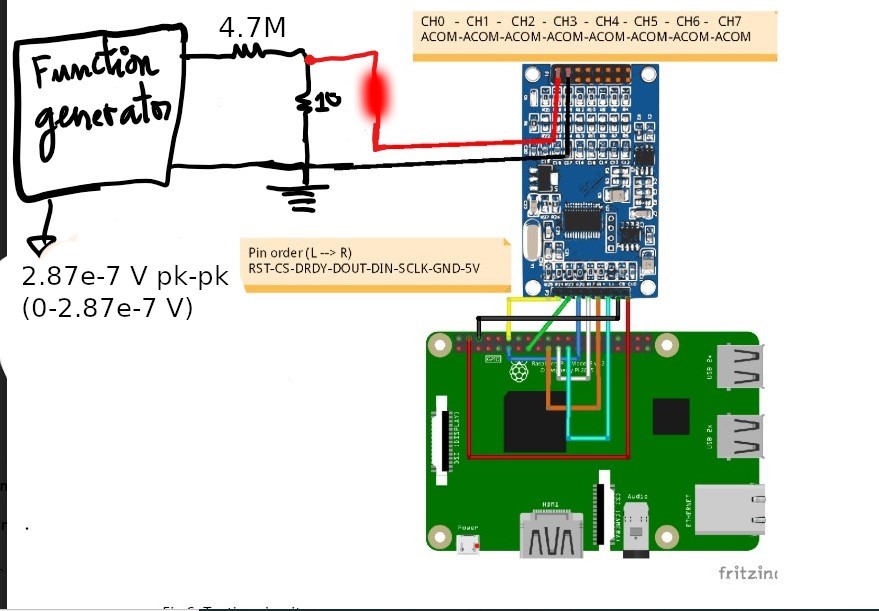
I generated a  sinusoidal 2Hz 135mV pk-pk voltage (with min value = 0V and max value = 135mV) using a function generator (SWF-7000). I'm using a voltage divider with one 10 Ohms resistor and a 4.7 Mega  Ohms to divide the signal. The output signal is taken on the 10 Ohms resistor so the the new signal should be 135mV*(10/(10 +4.78*10e6)) = 2.8723e-7V pk-pk voltage (with min value = 0V and max value = 2.8723e-7V). I'm sampling the 2.8723e-7V pk-pk with an ADS1256 with a sampling rate of 50SPS using the common mode and VREF = 2.5V, PGA = 1 with buffer OFF. The ADS1256 I'm using is implemented on the "High -Precision ADS1256 24-Bit 8 Channel ADC board"  https://www.amazon.com/High-precision-ADS1256-Channel-Digital-Converter/dp/B072C2LY17. I have attached the schematic of the board provided by the manufacturer. 

I keep having noisy reading whenever I try to read small signal in the order of micro volts. For some period of time, the signal is being read properly and some other time all I get noise. I'm not why this is happening. I first thought the problem was with the SPI frequency so I connected the DRDY pin to the oscilloscope and the frequency I read was 49.07Hz which is pretty to the 50Hz I'm expecting. Also, I'm not sure why the amplitude of the voltage on the pin is 2.64V pk-pk (is this normal?) I thought the amplitude voltage should be 5V pk-pk since I'm supplying 5V to the ADS1256.

The noise I'm talking about can be seen in the second image. For some period of time, the shape of the signal (sinusoidal) is the same as the expected signal but then I get a noise for a few seconds then it goes to normal. I'm not sure why I'm getting those noise interval.

Let me know if you need more information regarding this problem.

Thanks

Fig 1. Oscilloscope reading of DRDY pin (yellow signal) for a Date Rate of 50SPS 

Fig 2. Output Voltage on channel 0

Fig 3. Circuit Set up 

Schematic diagram.pdf

  • Hi User,

    I am looking into this issue and will respond in the next 1-2 days.

    -Bryan

  • Hi User,

    Just as a quick note, the signal you are trying to measure (0.287 µV) is below the level of the ADS1256 noise at G=1, 50 SPS, buffer off, which is 0.644µVRMS according to Table 4. Is there any reason you are not using a high gain given such a small input signal?

    Also, the 4.7MΩ resistor will contribute 1.31µVRMS at T=25C and BW = 22.1 Hz (the BW of the digital filter at DR=50SPS in Table 12). So this is already adding a lot of noise to your system, more so than your actual signal.

    Is there any reason you are dividing down your signal so much? This is certainly not helping your system's noise performance.

    -Bryan

  • Hi Bryan,

    For some reason, I have better performance (reading) whenever I use a gain 1. I also tried with buffer ON and it made everything even worse.

    The reason I'm using this voltage divider is generate a very small signal. The smallest voltage pk-pk my function generator can generate is 135mV pk-pk but I need smaller amplitude voltage in order of micro volts. Is there a better way of generating micro volts pk-pk signals from a milli volts pk-pk without using a voltage divider? 

    How did find the 1.31µVRMS noise at T=25C  that the 4.7MΩ resistor will contribute to the system?

  • Hi User,

    I don't think using a resistor divider is a bad way to reduce the signal amplitude, but in this particular case you are reducing the signal below the system noise floor, so you will not be able to measure it. Can you try making the signal larger and see if everything works okay? Maybe see if you can measure the original signal (135mV) and then work your way down from there. This will at least confirm your system is operating properly, and that this is simply a noise issue. You can also try sampling slower (e.g. 2.5 SPS) and with a higher gain (e.g. 64 V/V)

    The resistor noise equation is sqrt(4*Kb*T*R*F). You can find calculators on Google that will perform this calculation for you to determine the RMS voltage noise contributed by the resistor.

    -Bryan

  • HI Bryan,

    I've already tried larger voltages down to 10mV pk-pk and it seemed to work fine. Whenever I go smaller I get a lot of noise in the signal.

    I've also tried with a DC power source (GW Intek Programmable Power Supply PSP-405 ) and surprisingly I got the same behavior (PGA =1 gives me the best performance with buffer OFF). I fed a 0.01 V DC voltage to the  AIN0 and ACOM of the ADS1256  and according to the datasheet with PGA = 64 I should be to read ±78.125mV pk-pk but with this 0.01 V DC voltage, I'm reading the max count which is 0x7fffff or 8388607 with buffer OFF. I get this max count with PGA = 32 and 64 with buffer OFF.

    Is it normal that I have this kind of behavior when reading a DC value? 

  • Hi User,

    For the 10mV DC signal, do you get the same result with the buffer on?

    -Bryan

  • Hi Bryan,

    For the 10mV DC signal, I have relatively better reading with the buffer on. All PGA values from 1 to 64 (with buffer on) give me a value close to 0.0106V which is better than what I get with buffer off. With buffer off, I tend to have better reading when the date rate is high. For example, with PGA = 1 (with buffer off) and date rate = 100SPS, I get 0.0201V for a 10mV signal whereas with data rate of 30000SPS, I get 0.0186V which is strange because I was expecting to see a lot more noise on the signal with higher data rate.

    I  also noticed something strange. When I divide the 10mV DC signal with 10K and  and 4.7M (the output being taken on the the 10K resistor) I get the same reading which roughly 1.3010576367378235e-05 V (1397 in decimal or 0x575)(with buffer on). For this reading, I set PGA = 64 and data rate =10SPS (with buffer on). I was supposed to get 3.021148038e-5 I'm not sure what's the problem.

  • Hi User,

    I believe this relates back to the discussion we had about the ADC's input impedance with the buffer on versus the buffer off. For your system it seems necessary to keep the buffer on for best results, likely due to the large source impedance in your system. You should note that at the very least, the board you are using has a 100Ω /1kΩ resistor divider at each input. Even this by itself might cause significant error when you are using the ADS1256 with the buffer disabled. It will also scale your signals by about 90% compared to what you think you should get. Have you tried checking the voltages with an accurate DMM to determine what you are actually applying to the ADC inputs, and compare this to the ADC output result?

    Also, please keep in mind that with the buffer on, the ADS1256 absolute input range can only go down to 0V, which is close to the level of your input signal. I would suggest level-shifting the input signal to mid supply (or 1.5V if buffer = on). If the input signal is floating relative to the ADC, then you can apply the bias voltage to one of the other ADC inputs e.g. AIN1, then measure between AIN0 and AIN1. This will keep your inputs close to the midpoint of the ADC's input range, avoiding the nonlinear region of the buffer. I believe we discussed something similar in this e2e post.

    Are you performing any calibration after changing the gain or data rate settings? This is suggested on page 24 in the ADS1256. You can also enable the ACAL bit such that the device will perform a calibration after a WREG command that changes data rate, buffer or PGA settings. This is described at the bottom of page 26. A calibration could be useful, especially with such small signals.

    -Bryan

  • Hi Bryan,

    I did measure the signal going to the ADS1256 with a DMM and the value I'm reading on the DMM corresponds to what I'm getting with the ADS1256 (with buffer on, ACAL enabled, common mode). But I can only check close few mV which is the maximum resolution for my DMM.

    For all of my readings, I have the Auto-Calibration enabled. 

    If I do level-shift the signal to mid-supply as you suggest am I still going to be able to use PGA = 8 to 64? Since their pk-pk amplitude is less than 2.5V or 1.5V as you suggested (±0.625V for PGA = 8 means the range is from 0V to 1.25V if reference voltage = 2.5V)

    I also seem to have better performance when using common mode versus differential mode. I'm feeding a 0.01V DC common signal to the ADS1256 and I get 0.0105V using the common mode and 0.036V when using differential mode (PGA = 64 and Data rate = 10SPS, ACAL enabled and buffer ON, reference voltage = 2.5V). Is this normal? I thought differential reading should provide better accuracy than common mode. 

  • Hi User,

    I saw that you clicked thread resolved, so I hope that you have figured out what you needed to make your system work. But I did want to address your last concerns:

    Can you explain what you mean by common versus differential mode? The ADS1256 always takes measurements in a true differential manner (AINP - AINN), so this doesn't really apply to this ADC like it would with some SAR ADCs. Check out video 2.1 in the Precision Labs series that describes the different input signal types, in case my nomenclature is unclear. Measuring a ground-referenced input would be called a single-ended measurement - but the ADS1256 is a true differential input ADC, and its coding scheme reflects as such.

    For the setup, I am suggesting something as shown below. You would need to add a 1.5V offset from your function generator to the 10mV signal, as shown below. Then apply 1.5 V to AINN on the ADS1256 (this assumes the buffer is on). So when you apply +10mV, AINP = 1.6V and AINN = 1.5V, so the differential signal seen by the ADC is +10mV. You can then see how -10mV would be similarly generated.

    Again, you should generally try to stay away from the input limits on your devices, and it is best practice to keep your signals centered at the midpoint of the supply range (there are some exceptions to this, so you can consider this a general recommendation).

    If you have any more questions on this topic, please let me know. If you run into additional challenges, please start a new thread and we will assist you.

    -Bryan

  • Hi Bryan,

    In the datasheet, it says to "use AINCOM as common input and AIN0 through AIN7 as single-ended inputs" for single-ended measurement and to "use AIN0 through AIN7, preferably adjacent inputs" for differential measurements. What I mean by single-ended mode is actually single-ended measurement that is I use AINCOM as common input.

    The signal coming from the function generator is ground-referenced I assume that is why I have better performance when doing single-ended measurements versus differential measurements. 

    My confusion in the previous message was that I thought if I use an offset of 1.5 V one terminal is going to be at 1.51V and the other terminal will be at 0V (Ground) since the function generator generates ground-referenced signals. But now that you explained how the ADS1256 works I don't think there will be a problem.

    Thanks

  • Hi User,

    Thanks for confirming, looks like we were talking about the same thing then: single-ended measurements. Note that you cannot enable the buffer and take single-ended measurements, since any variation in the GND potential could violate the ADS1256's datasheet specs for absolute input range.

    If your signal coming from the function generator is ground-referenced then I agree you would not be able to level shift it as is. That is why you would need the 1.5V offset. Or, where adding a DC offset is not possible, you can use a level shift circuit such as this one using an inverting amp or this one using a non-inverting amp to bias the signal to a specific voltage. These circuits also attenuate the inputs as well e.g. for +/-10V inputs, that many ADCs cannot natively accept.

    -Bryan

  • Hi Bryan,

    I don't understand why I can't take single-ended measurements with the buffer enabled. Should the buffer be enabled only with differential measurements?

    My input signal to the ADS1256 has a high input impedance and I won't be able to properly read the signal with the buffer off.  If I connect the ground terminal (probe) of the signal generator to AINCOM is there still going to be a violation on the Ground potential?

    Thanks

  • Hi User,

    You can theoretically take single-ended (SE) measurements with the buffer enabled, but the input range is limited to exactly AGND in this mode as you can see below. So if there is any noise on the ground pin or other disturbance, you might be outside of the ADC's operating conditions. The device may still function in this configuration, but its behavior may not be deterministic and datasheet specs are not guaranteed.

    With the buffer disabled, there is slightly more headroom on the absolute input voltage (min), which is there to allow for some small variation in the ground-referenced signal. This is not really to measure signals below GND e.g. a +/-10mV signal centered at 0V.

    If you want to measure such an input, I would use one of the level-shifting techniques we previously discussed

    -Bryan