This thread has been locked.

If you have a related question, please click the "Ask a related question" button in the top right corner. The newly created question will be automatically linked to this question.

ADS54J60EVM: ADS54J60EVM

Part Number: ADS54J60EVM
Other Parts Discussed in Thread: ADS54J60, TSW54J60EVM, LMH5401

HI,

I have the evaluation board of of the ADS54J60 (these are actually 2 boards: one is with the A2D, the other is with the FPGA).

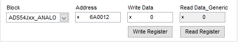
1. I want to test the BER of the ADC using the "ADS54Jxx GUI v1.6" and the "High Speed data converters Pro" programs.

I did not find how to do it. I saw an option to enable the test pattern but did not see any option to verify if all the data arrived correctly to the FPGA or not. I did not find a way to count BER errors.  How it can be done?

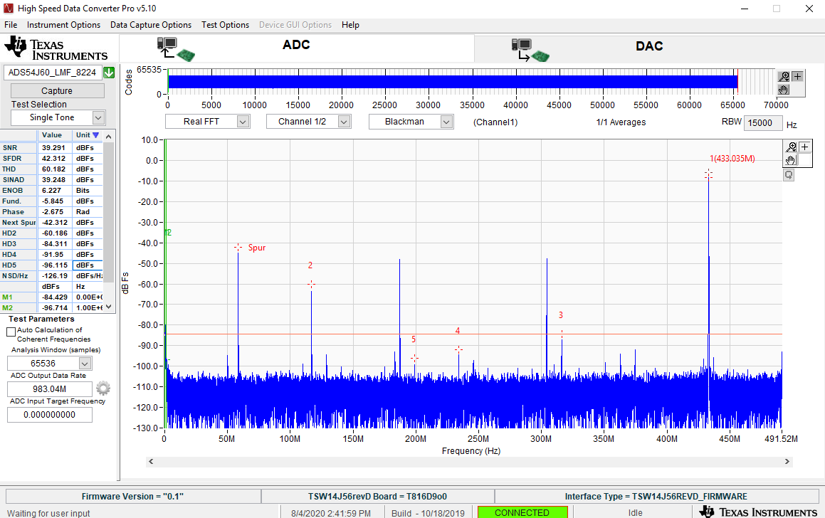
2. I saw that in the "High Speed data converters Pro" program, in the "instrument option" tab, under "SERDES test options" there is a way took at the eye and at the side there is a color BER bar. According the color it is hard to say if i had BER errors or not. Is there a way to read the BER counter and not to rely on the bar colors?

Thanks,

Yuval

  • Yuval,

    You can change digital gain, which would just increase or decrease the digital value (no effect on physical layer), you can change the JESD swing which will increase or decrease the actual serdes output amplitude, or change the de-emphasis setting, which will also effect the serdes physical output.  De-emphasis is a system process designed to decrease, (within a band of frequencies), the magnitude of some (usually higher) frequencies with respect to the magnitude of other (usually lower) frequencies in order to improve the overall signal-to-noise ratio by minimizing the adverse effects of such phenomena as attenuation distortion or saturation of recording media in subsequent parts of the system. This can be adjusted using page 0x6A00 addresses 12h-15h. 

    Both settings should help to some point. Try monitoring the EYE while making these changes.

    I would suggest you force the ADC to output continuous K28.5 characters using address 0x01 in page 6900 and see if you can observe these characters with a scope at the receiver.

    Regards,

    Jim

  • HI,

    I just want to make sure i am doing the right thing.

    According the data sheet, in page 0x6a00, register 12, bit 1, i must write 1. But when i read the register i got 0x0.

    Is it ok? should i read 0x0 although bit #1 should be '1' ?

    Yuval

  • Yuval,

    This bit is not readable. Do the write a "1" as mentioned in the data sheet.

    Regards,

    Jim

  • Hi Jim,

    I have made few more tests and i have few questions:

    1. I set the signal generator to 550MHz. I did not use any filter at the signal output. I see difference results between Ch A and Ch B. (i get ~6dB difference in SNR FS).. I attach the pictures. Can you explain why. 

    2. My application is running from DC to 400MHz. How can I convert the ADC eval board to support DC.

    Thanks,

    Yuval

  • HI Jim,

    1. I did the write '1' as mentioned in the data sheet but when i read the register i read the same value that i wrote (it means that this bit is readable) so i am not sure  that i wrote correctly to register 6A0012.

    2. In addition, i do not see any change in the eye when i run it in the "serdes test option"

    Yuval

  • Yuval,

    The TSW54J60EVM has amplifiers and an ADS54J60 that can be configured for DC application.

    In page 0x6A00 address 0x12, you need to change bits 2-7 to change the emphasis. Bit 1 must always be a "1" and writing a "1" will not show you anything with respect to the serdes eye.

    Regards,

    Jim

  • Hi Jim,

    I am trying to measure the ADC BW but the results i get are weird. this is what i did:

    1. The frequencies I measured were from 10MHz up to 600MHz.

    2. Each frequency, I first measured on Scope (just the signal generator + cable). The scope is 2GHz BW, 10GSPS.

    3. Then i measured the full set (signal generator + cable + eval board) by the HSDC tool

    4. The results i got from (3) I reduced with the results i got from (2) and converted to dB

    5. I attached the excel file with my measurements

    6. Looks like unstable results (see below)

    7. can you tell me what have i did wrong or explain the results.

    Thanks,

    Yuval

    ADS 54J60 BW measure.xlsx

  • Yuval,

    Not 100% sure what you are doing here. Are you comparing the analog input power with the digital output power of the ADC?

    What do you mean by in #4

    "4. The results i got from (3) I reduced with the results i got from (2) and converted to dB"

    Did you subtract one power number from the other?

    Regards,

    Jim

  • HI Jim,

    Since I want to measure the BW of the ADC only , I want to remove from the final result the BW influence of the signal generator + cable (they might also influence the result).

    This is what i do:

    1. I inject to the eval board several signals at different frequencies (10M, 50M, 100M, 150M,...., 600M) , all at 10dBm level.

    2. With the HSDC tool I capture the signal and look at the time domain. From the table I take the rms value (you can see how the value get smaller as the frequency increases). This is actually the BW behavior of the setup.

    3. Now, since the setup includes Signal generator + cable + A2D and I am interesting only in the ADC BW, then I want to remove the BW influence of the signal generator + cable

    4.  To do it, I used the same signal generator + cable and by scope I measured the rms value for each frequency (scope is 2GHz BW, 10GSPS). By this I actually measure the BW of the signal generator + cable

    5. Now I compensated the BW of the signal generator + cable from the results that I got by the HSDC tool to get only the A2D BW.

    I hope I clarified myself.

    Yuval

  • Yuval,

    Ripples can be seen from the source  as well. Can you try to add a 6 or 10db attenuator in the path near ADC?

    You may also want to do some tests with LPF filter removed (R14, C9, R9) on CHA.

    Also some of this could be related to the transformer. See attached data we captured with this EVM using different transformers.


    Regards,


    Jim

    2313.Passband Flatness Results 12_16_14.xlsx

  • HI Jim,

    1. According the excel you sent,, i see that the ADT1-1WT transformer gives bad results (BTW, there are 2 columns of ADT1-1WT. what's the difference between them)?

    2. If so then I prefer to remove the transformer and measure the BW. For this i need to do the following. Correct me if i am wrong:

    a. Assemble 0 ohm resistor on R3, R4, C1, C3

    b. Assemble J1

    c. Remove R6, R7, C6 and C7

    d. Need to add a SE-Diff amplifier (to connect the signal generator to J1 and J2). Do you have an eval board for this that you can ship me?

    3. The LPF that you mentioned  (R14, C9, R9), please send me its behavior?

    4. Does the transformer can influence other parameters like SNR?

    Yuval

  • HI Jim,


    I have one more question.

    I measured the floor noise of the ADC (input is connected to 50 ohm resistor) and I got ~6.5 LSB rms.

    when I calculated the floor noise according the ADC data sheet (Noise floor: –159 dBFS/Hz and Input bandwidth (3 dB): 1.2 GHz) I calculated ~17 lsb noise

    What am I missing? why the tests give much better result than the theoretical calculation?

    Yuval

  • Hi Yuval,

    The 6.5LSB rms is input referred noise? Is that your calculation for the LSB result?

    Regards,

    Rob

  • 1. According the excel you sent,, i see that the ADT1-1WT transformer gives bad results (BTW, there are 2 columns of ADT1-1WT. what's the difference between them)?

    The second column had the 5 Ohm series resistors replaced with 0 Ohms. 

    2. If so then I prefer to remove the transformer and measure the BW. For this i need to do the following. Correct me if i am wrong:

    a. Assemble 0 ohm resistor on R3, R4, C1, C3

    b. Assemble J1

    c. Remove R6, R7, C6 and C7

    d. Need to add a SE-Diff amplifier (to connect the signal generator to J1 and J2). Do you have an eval board for this that you can ship me?

    Correct. Contact the high speed amplifier forum regarding an eval board.

    3. The LPF that you mentioned  (R14, C9, R9), please send me its behavior?

    LPF around 2.5GHz

    4. Does the transformer can influence other parameters like SNR?

    Main effects are HD2 and HD3 which would effect SFDR.

    Regards,

    Jim

  • HI Rob,

    My calculation is for LSB.

    1. If the Noise floor is –159 dBFS/Hz and the Input bandwidth (3 dB) is 1.2 GHz then the total noise is: SQRT (10^(-159/10) * 1.2e9 * 1.57) = 487uV.

    2. Since the Input full-scale is 1.9 VPP then 1 LSB = 1.9 / 2^16 = 29uV

    3. 487 uV / 29 uV = 16.698 LSB

    These are my calculations but when I measure the ADC noise I got `6.5LSB which is far from the theoretical result.

    Yuval

  • HI,

    My system BW might be 200Mhz therefore I thought that in order to improve DR (Dynamic Range) I will use the by 2 decimation factor. I started to test it but I am not sure i used the correct files. The files i use are these:

    a. LMK_Config_Onboard_983P04_MSPS.cfg

    b. ADS54J60_2x_dec_lowpass_4222.cfg

    c. from the HSDC I chose the ADS54J60_2x_4222

    d. In the ADC output data range I wrote (491.52M)

    Questions:

    1. Are these the correct files to make decimation by 2 ? do you have a format or a description of the files names that it will be better understood?

    2. I connected the input to a 50 ohm termination to measure dark noise of the board. i captured data many times but sometimes I saw a spike on the signal (see attach). Can you explain this ?

    Yuval

  • Yuval,

    These settings are correct. See attached. The spike may be due to the offset correction algorithm. Try turning this off.

    Regards,

    Jim

    8357.ADS54J60EVM Quick Startup Guide 7_13_17.docx

  • Hi Jim,

    The offset correction algorithm is used for the interleave. Isn’t it ? what will be the impact of turning it off ?

    Yuval

  • Yuval,

    The device has two correction blocks. The interleave correction block corrects for gain/timing mismatches and the offset correction block corrects for DC offset. In most applications, a customer will use the device with AC coupling. In this case the offset correction will correct for small amounts of internal DC offset. If a user is set up for DC coupling, if there is a large DC component on the analog  input, the offset correction block will try to correct for this and possible causing spurs to show up. Is your board still set up for AC coupling? If so, I am not sure why you are seeing this spike. Does it go away when you remove the 50 Ohm termination?

    Make sure to always press the board reset after changing the LMK setting and before loading a new ADC configuration.  

    Regards,

    Jim 

  • Hi Jim,

    1. The eval is still AC coupling

    2. I am pressing the reset button after changing the LMK.

    3. I repeated the test without 50 ohm termination at the inputs (the inputs were left open) and I still see the spikes on both channels.

    Yuval

  • Hi,

    I have a question regarding the save raw data.

    When I save it I see that I get different numbers than in the capture.

    In the CSV file I get negative values (see attached example) while they for sure do not exist in the capture screen (in the capture screen the values are around 32K).

    Should I add 32K to the CSV file in order to be matched to the capture screen?

    Yuval

    noise.csv

  • Hi,

    About the spike that i saw when I measured noise.

    1. I tested it on DC coupled configuration - the spike exits

    2. It last 1 sample

    3. Its power is more than 1000 LSB

    4.; Attached excel files with data so you can check.

    YuvalSpike Ch A.csvSpike Ch B.csv

  • Yuval,

    HSDC Pro displays the numbers as unsigned binary and the csv file is saved as two's comp data. Just add 32k like you mentioned.

    Regards,

    Jim 

  • Yuval,

    I do not see these spikes with my setup when using bypass mode or low pass filter mode. Are these always located at the same frequency? Is there some test equipment running nearby your setup that might be causing this?

    Regards,

    Jim 

  • HI Jim,

    1. The spikes do not happen always but sometimes. Did you run it enough time ?

    2. There are no other instruments working around. Anyway, I will test it in another environment to see if it is repeated.

    3. Maybe it is related to the interleave calibration. Is this calibration happens automatically or should I operate it  ? what will be the impact If I had to operate it and I did not ?  

    Yuval

  • Hi Jim,

    I have an eval board of the FDA LMH5401. I want to connect it to the ADS54J60 (DC-coupled) and test the full channel.

    In order to make it right I will appreciate if you can send me guide lines (or a drawing) of how to connect them together for DC coupling measurements

    1. At the ADS54J60 eval board, I assembled 0 ohm resistor on R3, R4, C1, C3 and also assembled J1

    2. I also removed R6, R7, C6 and C7

    3. Should I leave R1, R13, R2, R5, R14, R9, C2 and C9 as is or should I remove them and put 100ohm resistors between AINM and AINP ?

    4. Should I connect the VCM from the ADC54J60 eval board to the VCM at the LMH5401 eval board ?

    5. What powers should I give to the LMH5401 eval board. I gave +/-2V, is it OK? do 0V and 5V are OK also?

    Thanks,

    Yuval

  • Yuval,

    For #1 and #2, that is correct. For #3, You can leave these in. For #4, yes. For #5, see the attached files. We have a TSW54J60EVM that uses this ADC with two amplifiers. The User's Guide has information regarding DC coupled applications with these parts.

    Regards,

    Jim

    2671.TSW54J60EVM-SCH_B.pdfslau649a.pdf