This thread has been locked.

If you have a related question, please click the "Ask a related question" button in the top right corner. The newly created question will be automatically linked to this question.

ADS1015: error result from ADS1015

Part Number: ADS1015

Hi Team:

could you help to take a issue below:

We get customer system and tested it recently. But the result is wired,
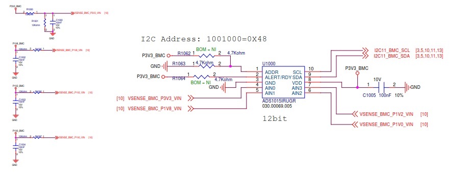
the design is as follows graph
image.png
AVIN0 monitors 3.3V, AVIN1:1.8V AVIN2:1.0V AVIN3:1.2V

Then for AVIN1: I set Config Register(offset 0x1) to 0xc383(single-shot) , then read offset 0x0 got 0xf0ff 
                             set Config Register(offset 0x1) to 0xc283(continuous) , then read offset 0x0 got 0xe0ff 

So as AVIN2:   Config Register(offset 0x1) to 0xd583(single-shot) , offset 0x0 got 0xf0ff 
                          Config Register(offset 0x1) to 0x4483(single-shot) , offset 0x0 got 0xe0ff 


The return value is not reasonable value for converting
Any incorrect setting or reading procedure I  misunderstand??
thanks!

  • Richard,


    With the register settings, here are the configurations that the device would have been set to, ignoring the comparator settings:

    C383h:
    AINP = AIN0 and AINN = GND
    FSR = ±4.096 V
    Single-shot mode or power-down state
    1600 SPS

    C283h:
    AINP = AIN0 and AINN = GND
    FSR = ±4.096 V
    Continuous-conversion mode
    1600 SPS

    D583h:
    AINP = AIN1 and AINN = GND
    FSR = ±2.048 V (default)
    Single-shot mode or power-down state (default)
    1600 SPS (default)

    4483h:
    AINP = AIN0 and AINN = GND
    FSR = ±2.048 V
    Continuous-conversion mode
    1600 SPS

    I'm not sure if the last one is correct because it's now set to measure AIN0 instead of AIN1. Regardless, the resulting value isn't correct.

    I would start by looking at the I2C communication between the master and the device. A read from the device should be a 5 byte communication, and I'd like to see all the communication, reading each of the bits within the I2C transaction. This can be done with an oscilloscope with some memory, but it might be easier with a logic analyzer. I'd also like to point out that because the ADS1015 is a 12-bit device, the last four bits should be 0000b. With the readings from the ADC that you posted, I'm curious if the first and second bytes were swapped. That doesn't explain why the value is off, but it might give some clues while debugging.

    Just in case, I would also try reading back the configuration register. It's a good test to make sure the read is happening properly.


    Joseph Wu

  • Richard,


    I haven't heard from you for a little while, so I thought I'd check on your customer's status. From my last post, I suggested that your customer check on the I2C communication and show a scope plot for it. I also suggested that they try to read back the configuration register, to ensure they are able to read back a known value.

    I'll close this post for now. If your customer continues to have problems with this, post back and we can continue to work on this again.


    Joseph Wu

  • Hi Joseph:

    could you help me on this?

    image.png

    Follow the spec command,

    I think we can access the ADS1015 registers, but we still have issue about return value.

     image.png

    The above is our SCH design:

    For AIN0: VSENSE_BMC_P3V3_VIN

    The measuring VSENSE_BMC_P3V3_VIN value is 1.781V

    Write to Config register:   Byte[0]=0x48 Byte[1]=0x1 Byte[2]=0xC2   Byte[3]=0x83 

    Write Command:    Byte[0]=0x48 Byte[1]=0x0

    Read Conversion register: Byte[0]=0x49 Byte[1]=0x4b Byte[2]=0x30 


    For AIN1: VSENSE_BMC_P1V8_VIN

    The measuring VSENSE_BMC_P1V8_VIN value is 1.194V

    Write to Config register:   Byte[0]=0x48 Byte[1]=0x1 Byte[2]=0xD4   Byte[3]=0x83 

    Write Command:    Byte[0]=0x48 Byte[1]=0x0

    Read Conversion register:  Byte[0]=0x49 Byte[1]=0x37 Byte[2]=0xf0  


    For AIN2: VSENSE_BMC_P1V0_VIN

    The measuring VSENSE_BMC_P1V0_VIN value is 0.981V

    Write to Config register:   Byte[0]=0x48 Byte[1]=0x1 Byte[2]=0xE4   Byte[3]=0x83 

    Write Command:    Byte[0]=0x48 Byte[1]=0x0

    Read Conversion register:  Byte[0]=0x49 Byte[1]=0x70 Byte[2]=0x10  


    For AIN3: VSENSE_BMC_P1V2_VIN

    The measuring VSENSE_BMC_P1V2_VIN value is 1.782V

    Write to Config register:   Byte[0]=0x48 Byte[1]=0x1 Byte[2]=0xF4   Byte[3]=0x83 

    Write Command:    Byte[0]=0x48 Byte[1]=0x0

    Read Conversion register:  Byte[0]=0x49 Byte[1]=0x3d Byte[2]=0xb0  


    After transfer the return value, 

    the AIN0 truly vol is: 1.781  count value is: 2.408

    the AIN1 truly vol is: 1.194  count value is: 0.895 

    the AIN2 truly vol is: 0.981  count value is: 1.793 

    the AIN3 truly vol is: 1.782  count value is: 0.987   


    It seems the return value is unreasonable, is there any config wrong??

  • Richard,


    I believe that the data is correct, but it's coming out in the wrong order. For your data results, here is what your customer is getting:
    ADC data:
    AIN0 measurement 4B3
    AIN1 measurement 37F
    AIN2 measurement 701
    AIN3 measurement 3DB

    However, I think the data should be in a different order, swapping the first and second and third and fourth:
    ADC data swapped:
    AIN0 measurement 37F - 895*4.096/2^11 = 1.790
    AIN1 measurement 4B3 - 1203*2.048/2^11 = 1.203
    AIN2 measurement 3DB - 1793*2.048/2^11 = 0.987
    AIN3 measurement 701 - 987*2.047/2^11 = 1.793

    These values are close to the expected values that the customer measured:
    Measured values:
    AIN0 measurement 1.781
    AIN1 measurement 1.194
    AIN2 measurement 0.981
    AIN3 measurement 1.782

    There are a few possibilities here:
    First, they could have these measurements swapped in the the code somehow. I haven't seen their code, but they should be able debug this for themselves. If they need to they can isolate one measurement at a time, by enabling only one channel and making sure they get the correct reading for it.

    Second, I recommend that they use the device in single shot conversion mode. I often recommend using single-shot conversion mode and then wait a specific time to read from the device.

    1. Program the configuration register to make a conversion with the proper configuration.
    2. Wait the data period + an extra 10% + 20us. This is the time it takes to make a conversion with 10% to account for variation in the internal clock and an extra 20us to wake up the device after the last conversion.
    3. Read the last data.
    4. Repeat from 1 to start the next channel.

    At a data rate of 1600SPS, this is a 708us wait time.

    If they are using multiple channels, I would not use continuous conversion mode. When the configuration is programmed, the configuration is not set until the conversion in progress is completed. This can lead to confusion over when the device receives the configuration, and when to collect data. Even if you use the ALERT/RDY pin to indicate the time of the conversion completion, continuous conversion mode is usually more confusing to implement.


    Joseph Wu