- Ask a related questionWhat is a related question?A related question is a question created from another question. When the related question is created, it will be automatically linked to the original question.
The ADS5409EVM (same as ADS5402EVM) appears to be driving the ADC’s SCLK, SDIO, and SDENB pins with 3.3V levels in violation of the ADC’s absolute maximum input voltage levels.
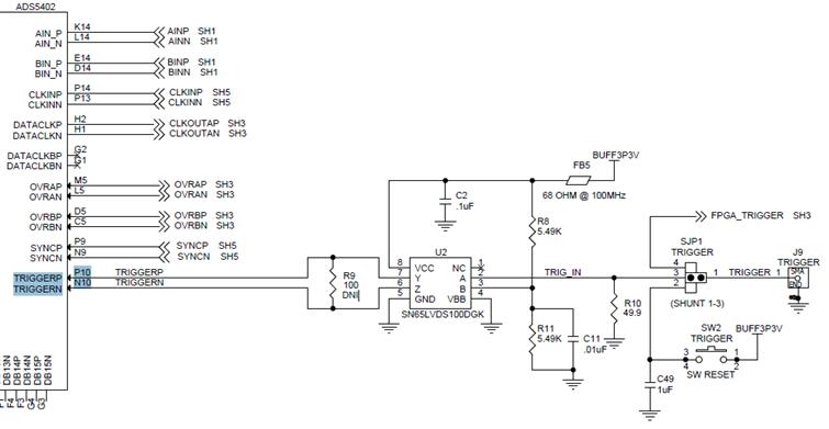
Here’s the relevant EVM circuitry at the ADC (SH6):
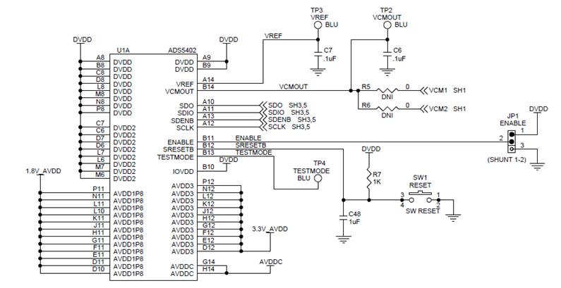
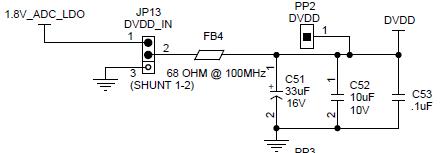
Note that the ADC’s IOVDD pin is tied to DVDD, which is sourced by the 1.8V LDO (SH4):
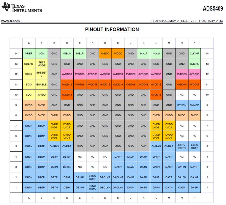
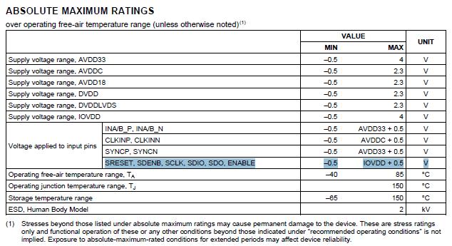
This appears to be a requirement per the ADS5409 datasheet (p.4):

The three pins in question, however, are controlled by an FT245R (EVM schematic, SH5):

Note that the VCCIO pin of the FT254R is tied to its own 3V3OUT pin (internal LDO). This puts the Voh levels between 2.2V and 3.2V (FT245R datasheet, p.16):

But the absolute maximum applied voltage for the three pins is IOVDD+0.5V (2.3V, assuming nominal IOVDD) (ADC datasheet p.5):
I’ll concede that, if the FT254R puts out minimum Voh levels (2.2V) they’d be just under the abs. max. rating of the ADC pins.
But even typical levels (2.7V) would be significantly in violation.
Can you clarify?