This thread has been locked.

If you have a related question, please click the "Ask a related question" button in the top right corner. The newly created question will be automatically linked to this question.

ADC32RF45EVM: Not getting Reference clock From the ADC32RF45 EVM

Part Number: ADC32RF45EVM
Other Parts Discussed in Thread: ADC32RF45, LMX2582, LMK04828, , ADC32RF80

Hello Sir,

We are using ADC32RF45 EVM board to Polarfire Tranceiver.

Input RF frequency : 150 MHZ from Signal generator

OSCin : 122.88 MHZ

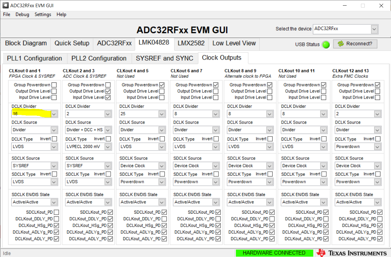
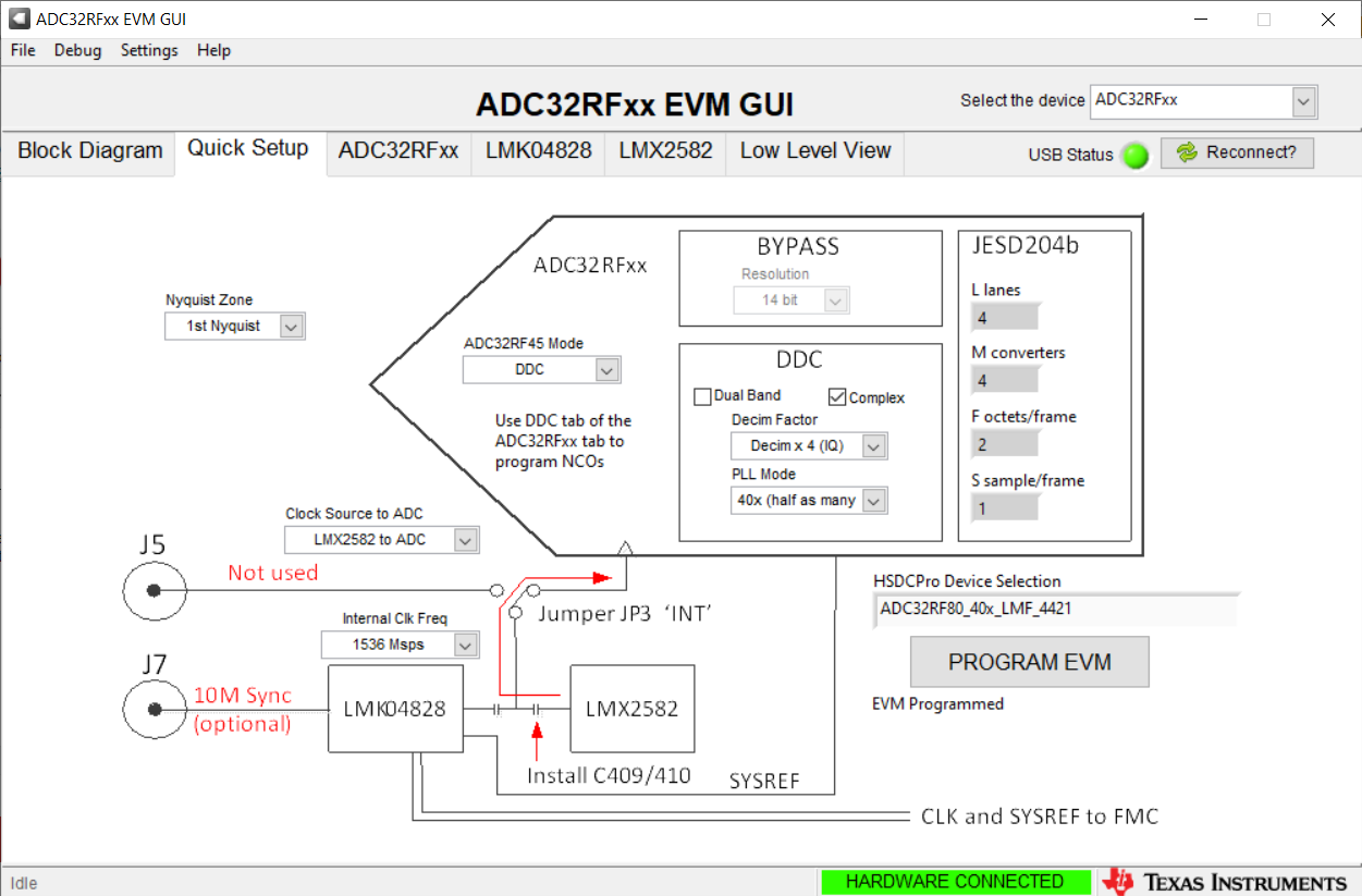
Clock source is LMX2582 to ADC is 1536Msps

As per datasheet of ADC, LMFS = 4421

DDC single band with complex ouput 

In JESD204b configuration is k=8
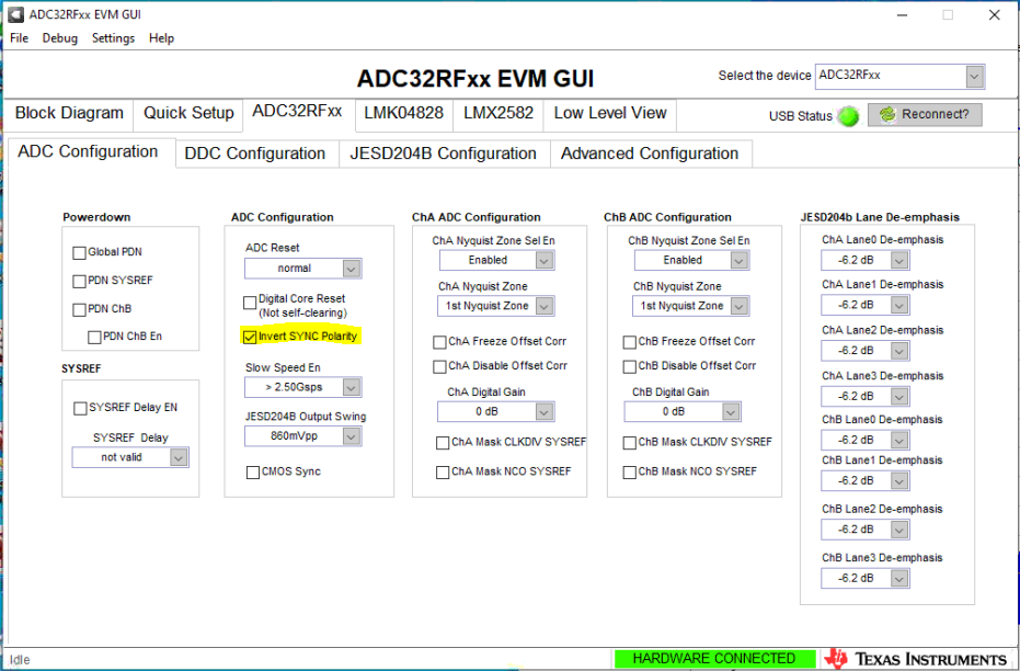
sync is requested

k28.5 mixed ADC

For LMK0408 ouput clocks section : divide by 8

please can you suggest me to get reference clock to ADC and SYNC and SYSREF generation

Thanks

Roja Veereddy

  • Hi Roja,

    What is the decimation factor you are using? 

    Do you see LED D4 (PLL2 locked) is ON after programming the EVM? This green LED is supposed to turn ON after LMK is programmed.

    For 1536 MSPS modes, when using TSW14J56EVM, after clicking "PROGRAM EVM" button, before capturing in HSDC Pro, to set the FPGA output clock correctly, DCLK divider for "CLKout 0 and 1" (in "Clock Outputs" tab in "LMK04828" tab as shown below) has to be doubled. 

    Regards,

    Vijay

  • Hello sir

    We are using decimation factor is x4

    we are using PLL mode is 40x

    During programming of EVM, PLL2 has locked and LED has become green. 

    please suggest us to get reference clock to FPGA from LMK04828

    i have tested with clock divided by 16 but we did not get reference clock. 

    Thanks

    Roja Veereddy

  • Hi Roja Veereddy,

    I have verified this mode on ADC32RF45EVM with TSW14J56EVM. I was able to capture ADC output data in HSDC Pro using ADC32RF80_40x_LMF_4421 (in select ADC drop-down menu). This means that 192M FPGA JESD clock is received by TSW14J56EVM.

    EVM GUI configuration screenshots:

    After you click "PROGRAM EVM" button, before capturing in HSDC Pro, to set the FPGA output clock correctly for 1536 MSPS, double DCLK divider for "CLKout 0 and 1" in "Clock Outputs" tab in "LMK04828" tab as shown below. 

    You also mentioned that LED D4 turned ON (green) during the programming, so the LMK PLL 2 is locked to 3072 MHz. With /16 divider, DCLKOUT0 output should be a 192 MHz clock.This clock net name is 'FPGA_JESD_CLKP/M' in the ADC32RF45EVM schematic  This clock is connected to FMC pins D4 and D5. Please double check if correct pins are being probed.

    Regards,

    Vijay

  • Hello sir

    We are using polarfire FPGA .

    In that we are using Tranceiver IP and JESD204b RX IP.

    In the Tranceiver IP:

    We have given RX data rate is 5Gbps

    CDR Reference clock frequency is 125 MHZ.

    In the JESD204b IP:

    We have given LMFS is 4 4 2 1

    K = 9

    Converter resolution is 16

    Total no of bits per sample is : 16

    Is there any change is require to get output.

    I am trying to see an output in chipscope, i am not finiding sync and JESD204b RX output CGS error is giving "1111"

    Sync is not coming 

    Please, could you suggest me to do any changes in those configuration, beacuse i have given pins properly and i have set GUI configuration properly still i didn't get data and sync.

    Thnaks

    Roja Veereddy

  • Hi Roja Veereddy,

    For this mode, Rx lane rate is 7.68 Gbps and K programmed by GUI is 16 by default. 

    Lane rate calculation can be found in the e2e thread below:

    Please also note that SYNCB polarity is inverted by default by GUI configuration. It can be changed using the below highlighted check-box in the GUI.

    Regards,

    Vijay